
Method for fabrication of a semiconductor device and structure
a semiconductor device and fabrication method technology, applied in the direction of pulse technique, instruments, computation using denominational number representation, etc., can solve the problems of increasing the cost of product development, the mask set cost required for each new process technology has been increasing exponentially, and the cost of improvement does come with a price, so as to reduce the high cost of manufacturing, reduce the cost of mask set cost, and reduce the effect of flexibility
- Summary
- Abstract
- Description
- Claims
- Application Information
AI Technical Summary
Benefits of technology
Problems solved by technology
Method used
Image

Examples
Embodiment Construction
[0134]Embodiments of the present invention are now described with reference to FIGS. 1-68, it being appreciated that the figures illustrate the subject matter not to scale or to measure.
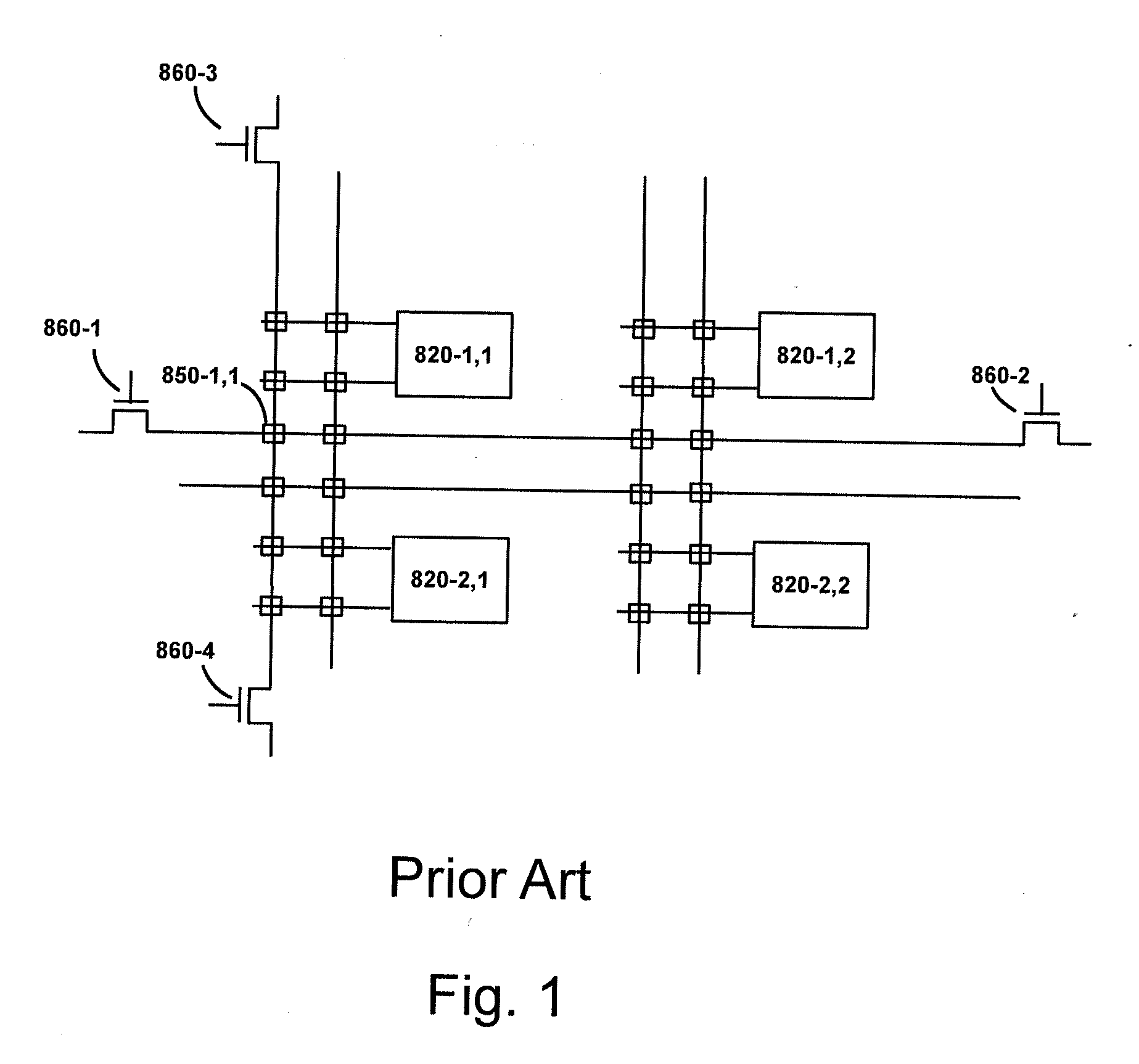
[0135]FIG. 1 illustrates a circuit diagram illustration of a prior art, where, for example, 860-1 to 860-4 are the programming transistors to program antifuse 850-1,1.
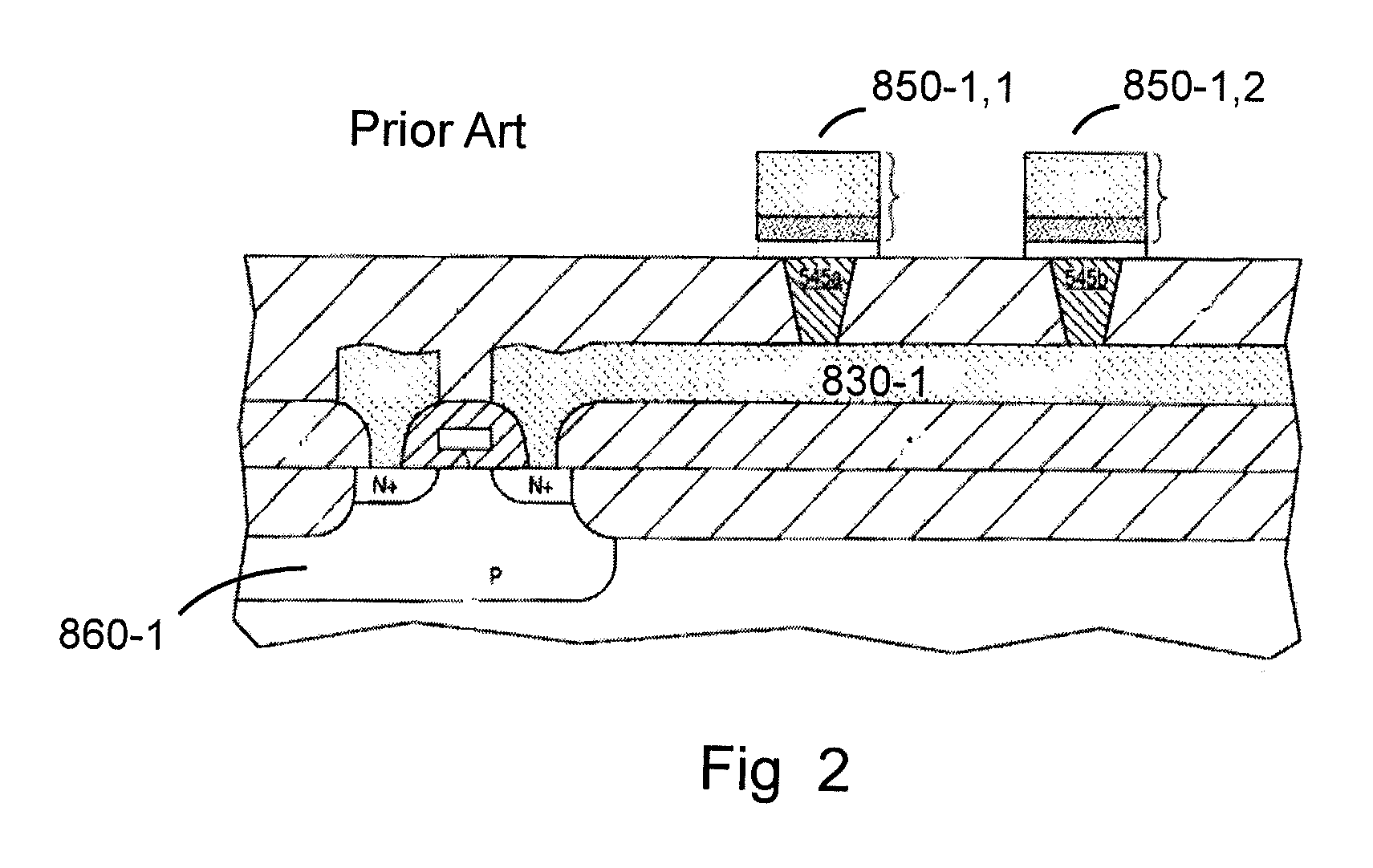
[0136]FIG. 2 is a cross-section illustration of a portion of a prior art represented by the circuit diagram of FIG. 1 showing the programming transistor 860-1 built as part of the silicon substrate.
[0137]FIG. 3A is a drawing illustration of a programmable interconnect tile. 310-1 is one of 4 horizontal metal strips, which form a band of strips. The typical IC today has many metal layers. In a typical programmable device the first two or three metal layers will be used to construct the logic elements. On top of them metal 4 to metal 7 will be used to construct the interconnection of those logic elements. In an FPGA device the logic eleme...
PUM
 Abstract
Description
Claims
Application Information