Target for a sputtering process for making a compound film layer of a thin solar cell, method of making the thin film solar cell, and thin film solar cell made thereby

a technology of compound film layer and target, which is applied in the direction of sustainable manufacturing/processing, final product manufacturing, conductors, etc., can solve the problems of reducing the efficiency of the solar cell, unhomogeneous size distribution of grains, and electricity loss, and achieve the effect of improving electric properties

Inactive Publication Date: 2011-03-31
LAI CHIH HUANG
View PDF4 Cites 29 Cited by
  • Summary
  • Abstract
  • Description
  • Claims
  • Application Information

AI Technical Summary

Benefits of technology

[0016]Therefore, an object of the present invention is to provide a target adapted for a sputtering

Problems solved by technology

When the carriers are transmitted along the normal direction in the compound film layer 13, they are liable to be scattered and trapped due to the existence of the grain boundary, which results in electricity loss and reduces the efficiency of the solar cell.
As shown in FIG. 2, the shape of the grains is irregular and the size distribution of the grains is not uniform.
The problem of electricity loss du

Method used


Image

  • Target for a sputtering process for making a compound film layer of a thin solar cell, method of making the thin film solar cell, and thin film solar cell made thereby
  • Target for a sputtering process for making a compound film layer of a thin solar cell, method of making the thin film solar cell, and thin film solar cell made thereby
  • Target for a sputtering process for making a compound film layer of a thin solar cell, method of making the thin film solar cell, and thin film solar cell made thereby

Examples


Embodiment Construction

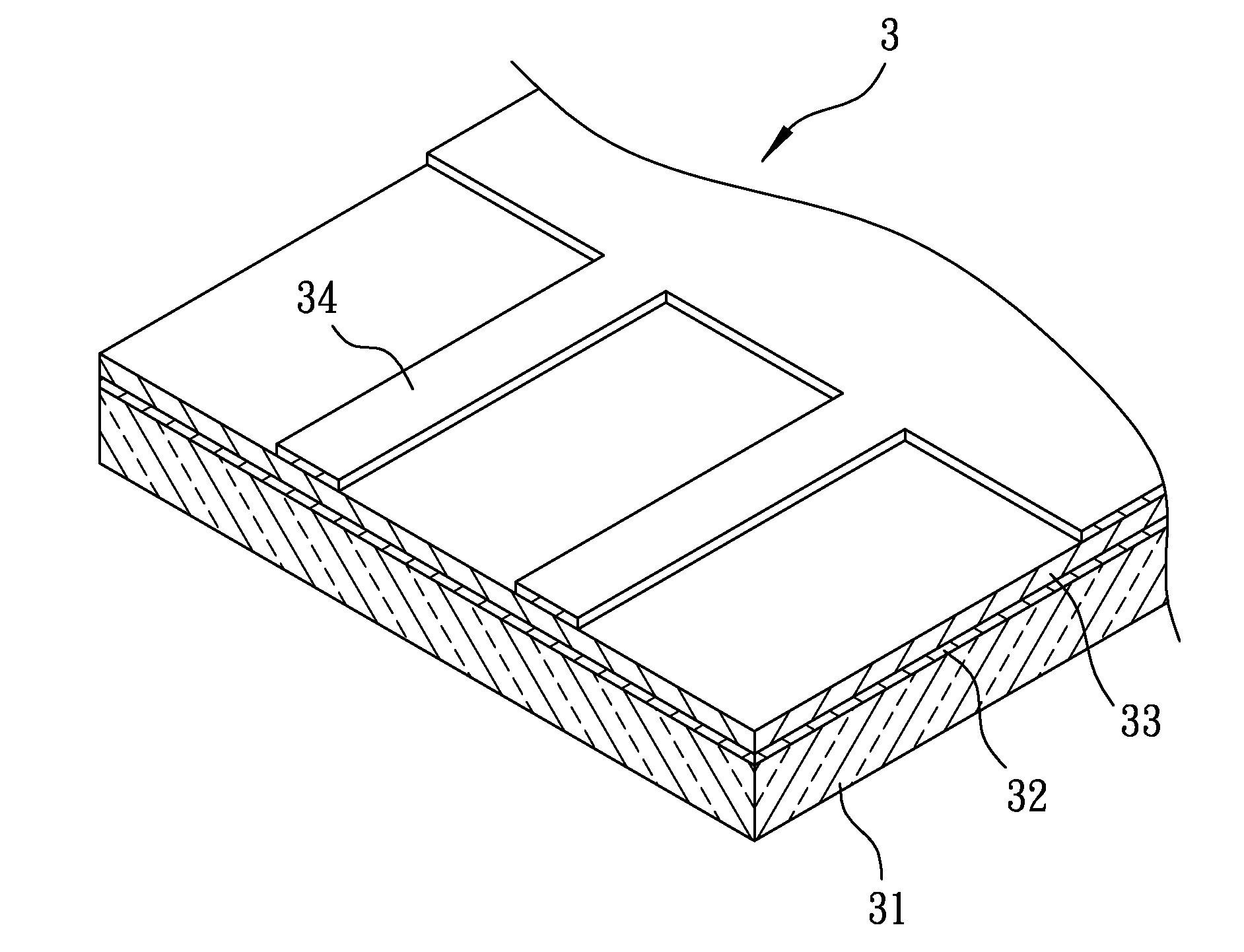
[0033]Referring to FIGS. 3 and 4, the first preferred embodiment of a method of making a thin film solar cell according to this invention is shown to include the steps of:

[0034]A) cleaning a substrate:[0035]A substrate 31 is provided and is washed and dried according to a process commonly used in the art. The substrate 31 suitable for the present invention may be glass, a flexible foil of metal or alloy, or a polymer. In this preferred embodiment, soda glass is used for the substrate 31.

[0036]B) depositing a back electrode:[0037]A back electrode 32 is deposited on the substrate 31 by a sputtering system using a first conductive material as a target. In this preferred embodiment, the first conductive material used as the target is molybdenum.

[0038]C) depositing a compound film layer:[0039]A compound film layer 33 is deposited on the back electrode 32 by a sputtering system using a target at a work temperature ranging from 150 to 600° C. The target used in this step includes a composi...


PUM

PropertyMeasurementUnit
Temperatureaaaaaaaaaa
Pressureaaaaaaaaaa
Pressureaaaaaaaaaa

Abstract

A target adapted for a sputtering process for making a compound film layer of a thin film solar cell includes a composition having a formula of CuB1-xCxSeyS2-y, wherein B and C are independently selected from Group IIIA elements; x ranges from 0 to 1; and y ranges from 0 to 2. A thin film solar cell made by sputtering using the target and a method of making the thin film solar cell are also disclosed. Specifically, the thin film solar cell includes a compound film formed with substantially columnar grains. The energy gap of the compound film layer may be varied using different work pressures during a sputtering process. At least one interlayer may be included in the compound film layer to control the size of columnar grains in the compound film layer.

Description

CROSS-REFERENCE TO RELATED APPLICATION[0001]This application claims priority of Taiwanese Application No. 098132508, filed on Sep. 25, 2009. The contents of the preceding application are hereby incorporated in its entirety by reference into this application.BACKGROUND OF THE INVENTION[0002]1. Field of the Invention[0003]The invention relates to a target for a sputtering process, more particularly to a target for a sputtering process for making a compound film layer of a thin film solar cell. The invention also relates to a method of making the thin film solar cell and the thin film solar cell made by the method.[0004]2. Description of the Related Art[0005]Among various thin film solar cells, CIGS (copper indium gallium diselenide) thin film solar cell is most valuable because of its properties, such as high photoelectric efficiency, light absorption ranging from 1.02 eV to 1.68 eV, light absorption rate (α) of more than 104-105 cm−1, a photoelectric material thickness that is less t...

Claims


Application Information

Patent Timeline
IPC IPC(8): H01L31/0272H01B1/02C23C14/14C23C14/34
CPCC23C14/0623C23C14/3414C23C14/3492H01L21/02485H01L21/02491Y02E10/541H01L21/02568H01L21/02631H01L31/0322H01L31/065H01L31/0749H01L21/02502Y02P70/50
Inventor LAI, CHIH-HUANGCHEN, CHIA-HSIANGCHEN, YI-CHANG
Owner LAI CHIH HUANG
Why Eureka
Try Eureka