Pixel, display device using the same, and driving method thereof

a technology of display device and pixel, which is applied in the direction of electric digital data processing, instruments, computing, etc., can solve the problems of deterioration of image quality and variation of oleds of one pixel, and achieve high image quality, high resolution, and high quality display

Active Publication Date: 2011-08-11
SAMSUNG DISPLAY CO LTD
View PDF3 Cites 54 Cited by
  • Summary
  • Abstract
  • Description
  • Claims
  • Application Information

AI Technical Summary

Benefits of technology

[0043]According to exemplary embodiments of a pixel, a display device including the same, and a driving method thereof, sufficient time to compensate the threshold voltage of the driving transistor may be obtained under high resolution and high frequency driving to realize a display device of high image quality. Accordingly, in embodiments of the driving circuit of the pixel using the high resolution and high frequency driving method, the compensation period of the threshold voltage of the driving transistor is sufficient such that each of the plurality of pixels of an exemplary display device has a complete threshold voltage compensation capability. Thus, the display device may realize a high quality display.

Problems solved by technology

This, in turn, may cause luminance variation of the OLEDs from one pixel to another.
In this case, however, it may be difficult to ensure that the time that the threshold voltage of the driving transistor of each pixel is compensated is sufficient, such that the image quality may be deteriorated.

Method used


Image

  • Pixel, display device using the same, and driving method thereof
  • Pixel, display device using the same, and driving method thereof
  • Pixel, display device using the same, and driving method thereof

Examples


Embodiment Construction

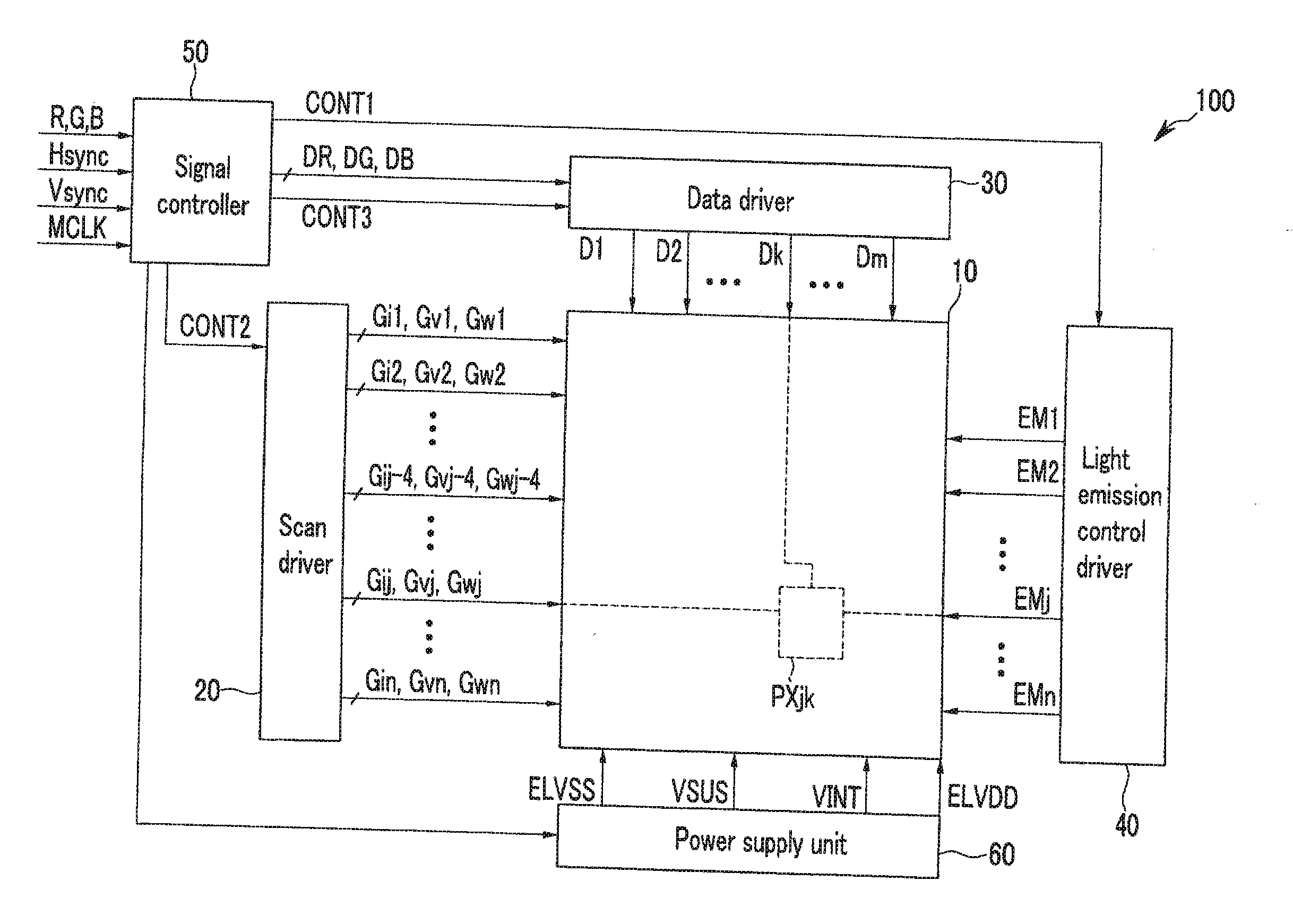
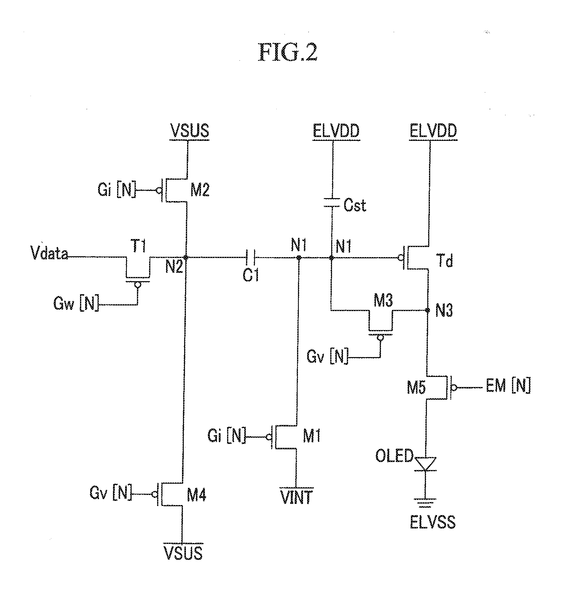
[0051]The present invention will be described more fully hereinafter with reference to the accompanying drawings, in which exemplary embodiments of the invention are shown. As those skilled in the art would realize, the described embodiments may be modified in various different ways, all without departing from the spirit or scope of the present invention.

[0052]Constituent elements having the same structure throughout multiple embodiments are denoted by the same reference numeral and are described in a first embodiment. In later embodiments, descriptions of these same constituent elements may be omitted. In addition, to clarify description of embodiments of the present invention, parts not related to the description may be omitted. In addition, like reference numerals designate like elements and similar constituent elements throughout the specification. Further, power sources and their corresponding voltages may be referred to with the same reference name where the appropriate meanin...


PUM


Abstract

A pixel, a display device using the same, and a driving method thereof are disclosed. According to exemplary embodiments of the pixel, the display device including the same, and the driving method thereof, sufficient time to compensate the threshold voltage of the driving transistor of the pixel may be obtained under high resolution and high frequency driving to realize a display device of high image quality.

Description

CROSS-REFERENCE TO RELATED APPLICATION[0001]This application claims priority to and the benefit of Korean Patent Application No. 10-2010-0012464, filed in the Korean Intellectual Property Office on Feb. 10, 2010, the entire content of which is incorporated herein by reference.BACKGROUND[0002]1. Field[0003]Aspects of embodiments according to the present invention relate to a pixel, a display device including the same, and a driving method thereof.[0004]2. Description of the Related Art[0005]Various kinds of flat display devices that are capable of reducing detriments of cathode ray tube (CRT) devices, such as their heavy weight and large size, have been developed in recent years. Such flat panel display devices include liquid crystal displays (LCDs), field emission displays (FEDs), plasma display panels (PDPs), and organic light emitting diode (OLED) displays. Among these flat panel display devices, the OLED display, which uses OLEDs to generate light by a recombination of electrons ...

Claims


Application Information

Patent Timeline
Patent Type & Authority Applications(United States)
IPC IPC(8): G06F3/038G09G3/30
CPCG09G3/3233G09G2300/0819G09G2320/043G09G2300/0861G09G2310/0262G09G2300/0852
Inventor HAN, SAM-IL
Owner SAMSUNG DISPLAY CO LTD
Why Eureka
Try Eureka