

Semiconductor device and manufacturing method thereof
a semiconductor and manufacturing method technology, applied in semiconductor devices, instruments, electrical devices, etc., can solve the problems of difficult to recognize display and display in the environment with strong external light, and achieve the effects of bright and high-quality display, less variation in characteristics, and high productivity
- Summary
- Abstract
- Description
- Claims
- Application Information
AI Technical Summary
Benefits of technology
Problems solved by technology
Method used
Image

Examples
embodiment 1
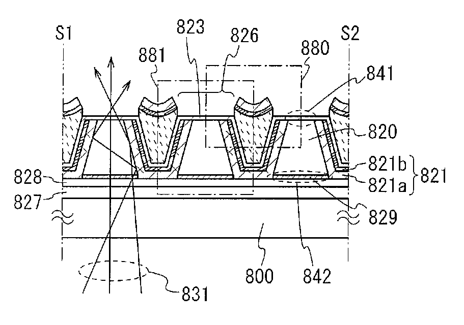
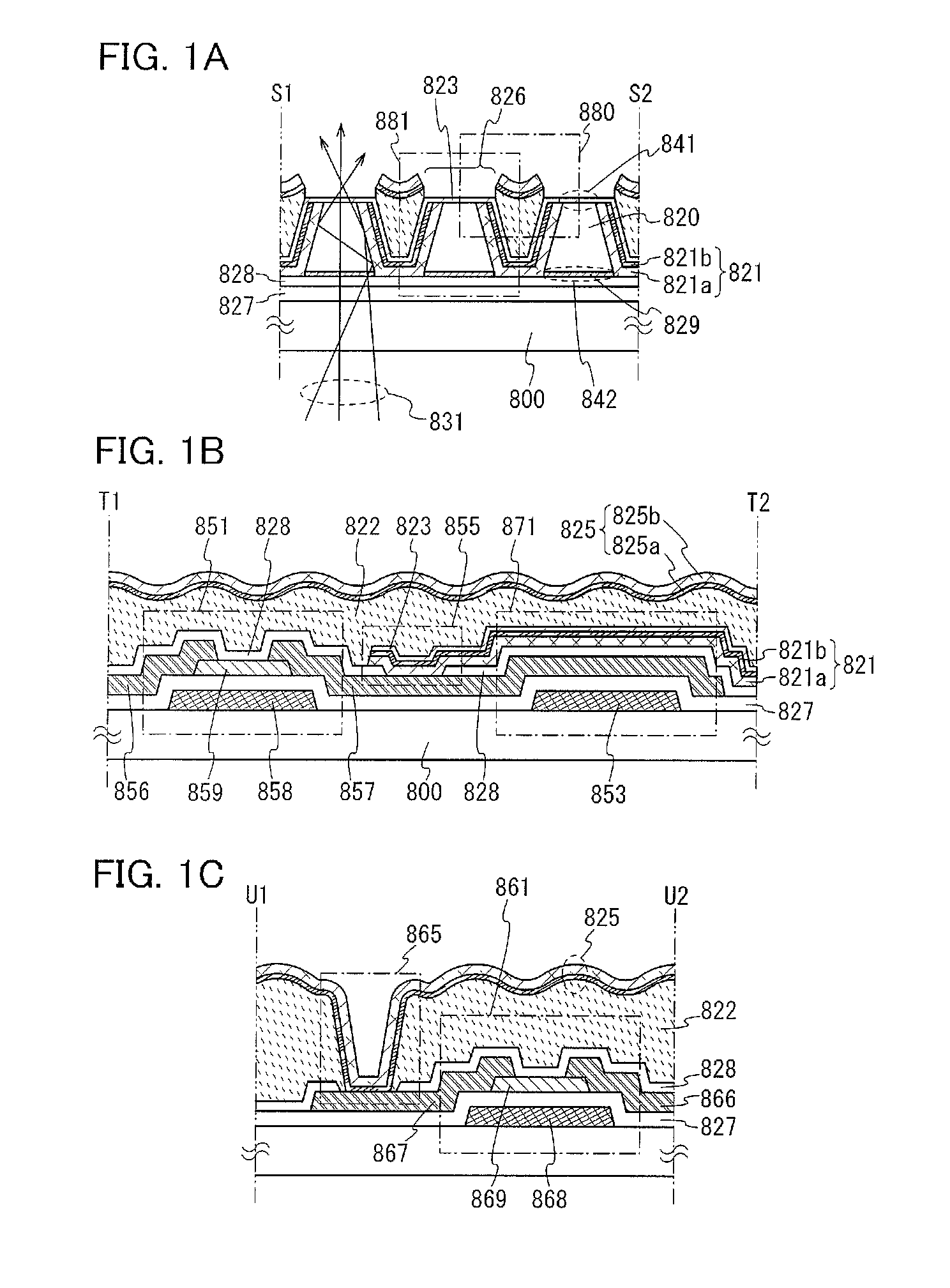
[0066]In this embodiment, a pixel structure which enables an increase in the amount of reflected light and transmitted light per one pixel in a semi-transmissive liquid crystal display device and a manufacturing method thereof will be described with reference to FIGS. 1A to 1C, FIGS. 2A and 2B, FIG. 3, FIGS. 4A to 4C, FIGS. 5A to 5C, FIGS. 6A and 6B, FIGS. 7A to 7C, FIGS. 8A to 8C, FIGS. 9A to 9C, and FIGS. 10A and 10B.
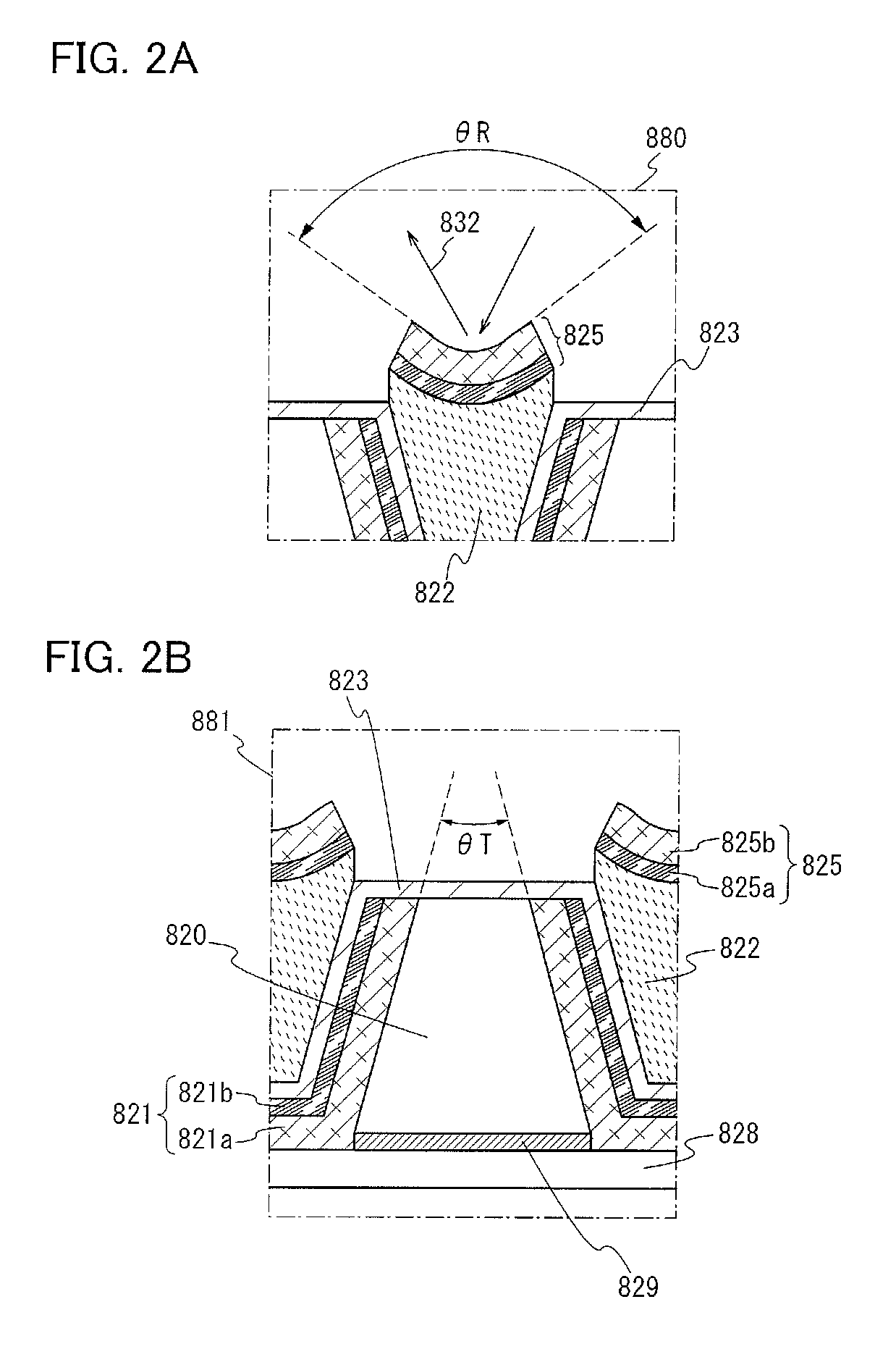
[0067]FIGS. 1A to 1C and FIGS. 2A and 2B illustrate cross-sectional structures of a pixel described in this embodiment. FIG. 3 illustrates a plane structure of the pixel described in this embodiment. FIGS. 1A to 1C illustrate cross-sectional structures of a portion along S1-S2, a portion along T1-T2, and a portion along U1-U2, respectively, denoted by clashed lines in FIG. 3. FIG. 2A is an enlarged view of a portion 880 in FIG. 1A. FIG. 2B is an enlarged view of a portion 881 in FIG. 1A.
[0068]The pixel described in this embodiment includes a transparent electrode 823 ...
embodiment 2
[0176]In this embodiment, an example of a transistor that can be applied to a liquid crystal display device disclosed in this specification is described. There is no particular limitation on the structure of the transistor; for example, a staggered type transistor or a planar type transistor having a top-gate structure or a bottom-gate structure can be employed. Further, the transistor may have a single gate structure including one channel formation region, a double gate structure including two channel formation regions, or a triple gate structure including three channel formation regions. Alternatively, the transistor may have a dual-gate structure including two gate electrodes positioned above and below a channel region with gate insulating layers provided therebetween. Note that examples of cross-sectional structures of transistors illustrated FIGS. 11A to 11D are described below. Transistors illustrated in FIGS. 11A to 11D are transistors each using an oxide semiconductor as a s...
embodiment 3
[0188]In this embodiment, a structural example of a semi-transmissive liquid crystal display module will be described. The semi-transmissive liquid crystal display module described in this embodiment displays images in mono-color display when used in a reflective mode, and displays in full-color display when used in a transparent mode.
[0189]FIG. 12 illustrates a structure of a liquid crystal display module 190. The liquid crystal display module 190 includes the backlight portion 130, the display panel 120 in which liquid crystal elements are arranged in matrix, and a polarizing plate 125a and a polarizing plate 125b which are provided with the display panel 120 positioned therebetween. The backlight portion 130 is a surface-emitting backlight portion that emits uniform white light. For example, the backlight portion 130 may include a white LED 133 placed in an end portion of a light guide plate and a diffusing plate 134 provided between the light guide plate and the display panel 12...
PUM
 Abstract
Description
Claims
Application Information