Three dimensional semiconductor memory devices
- Summary
- Abstract
- Description
- Claims
- Application Information
AI Technical Summary
Benefits of technology
Problems solved by technology
Method used
Image


Examples
Embodiment Construction
[0042]The embodiments of the inventive concept will now be described more fully hereinafter with reference to the accompanying drawings.
[0043]Similarly, it will be understood that when an element such as a layer, region or substrate is referred to as being “on” another element, it can be directly on the other element or intervening elements may be present. The same reference numerals or the same reference designators may be used to denote the same or substantially the same elements throughout the specification and the drawings.
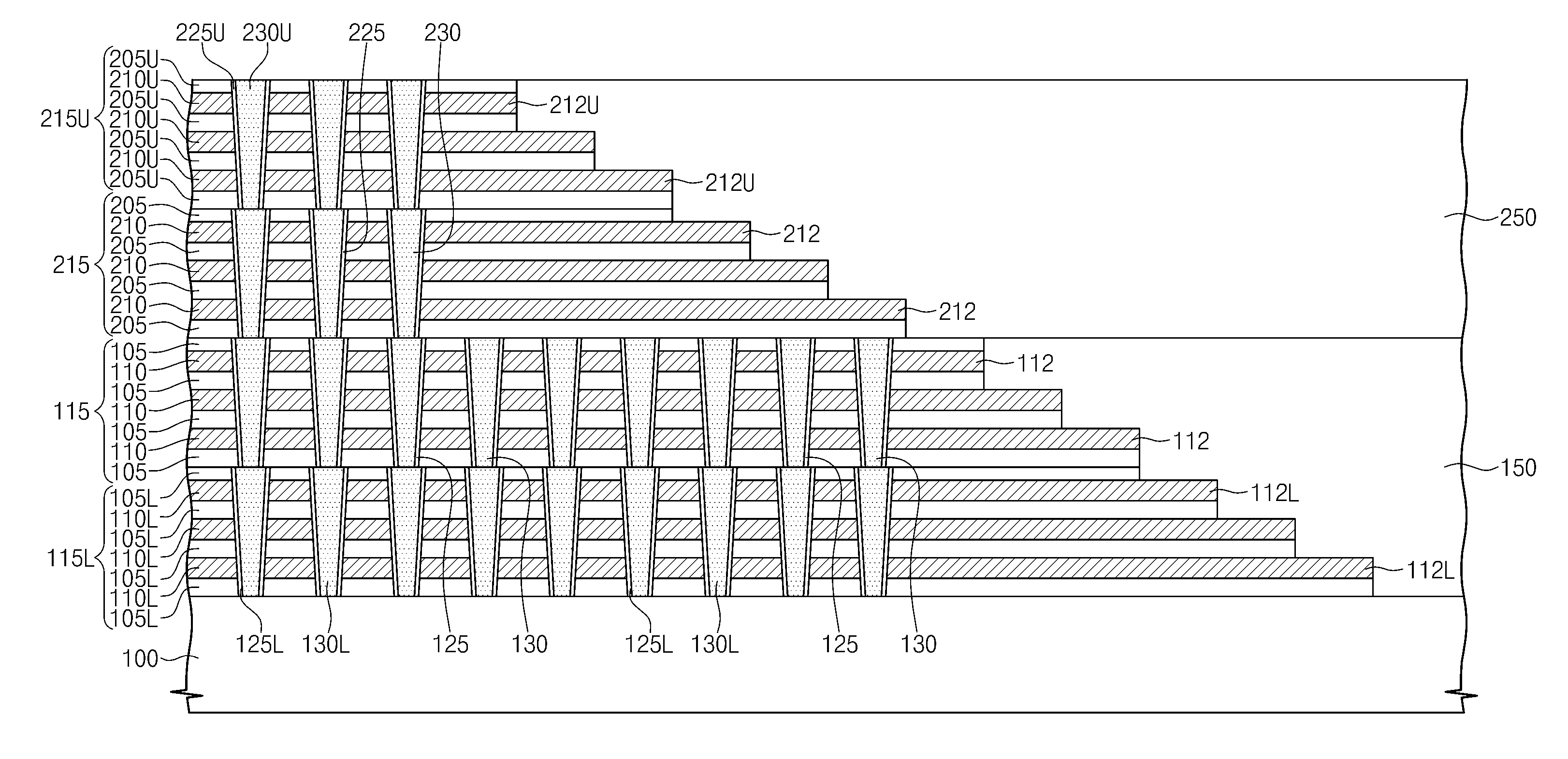
[0044]FIG. 1 is a cross sectional view illustrating a three dimensional semiconductor memory device according to an exemplary embodiment of the inventive concept.
[0045]Referring to FIG. 1, a plurality of stacked structures 115, 215, 315 and 415 may be sequentially stacked on a semiconductor substrate 100 (hereinafter, referred to as a substrate). A first stacked structure 115 may be disposed on the substrate 100. The substrate 100 may include a silicon substra...
PUM
 Abstract
Description
Claims
Application Information