Method for fabricating the flexible electronic device

Active Publication Date: 2013-01-10
HANNSTAR DISPLAY CORPORATION
View PDF7 Cites 52 Cited by
  • Summary
  • Abstract
  • Description
  • Claims
  • Application Information

AI Technical Summary

Benefits of technology

[0011]The disclosure provides a method for fabricating the flexible electronic devices, comprising: providing a first rigid carrier substrate and a second rigid carrier substrate disposed oppositely to each other, wherein at least one flexible electronic device is formed between the first rigid carrier substrate and the second rigid carrier substrate, and a plurality of first de-bonding areas, a first flexible substrate, the flexible electronic device, a second flexible substrate, a plurality of second de-bonding areas and the second rigid carrier substrate are formed on the first rigid carrier substrate; performing a first cutting step to cut through the first de-bonding areas, wherein the first de-bonding areas are divided into a first portion and a second portion, and the flexible electronic device is formed on the first portion of the first de-bonding areas; separating the first rigid carrier substrate from the first portion of the first de-bonding areas; removing the first rigid carrier substrate from the first portion of the first de-bonding areas to expose the first portion of the first de-bonding areas; and performing a second cutting step to cut through the second de-bonding areas, wherein the second de-bonding areas are divided into a third portion and a fourth portion, and the flexible electronic device is formed on the third portion of the second de-bonding areas; separating the second rigid carrier substrate from the third portion of the second de-bonding areas; and removing the second rigid carrier substrate from the third portion of the second de-bonding areas.

Problems solved by technology

When the flexible electronic devices are fabricated by a sheet-to-sheet process, and the flexible electronic devices are formed between two rigid carrier substrates, performing a process to a surface of the flexible electronic devices and taking the flexible electronic devices out of the two rigid carrier substrates are challenges.

Method used


Image

  • Method for fabricating the flexible electronic device
  • Method for fabricating the flexible electronic device
  • Method for fabricating the flexible electronic device

Examples


first embodiment

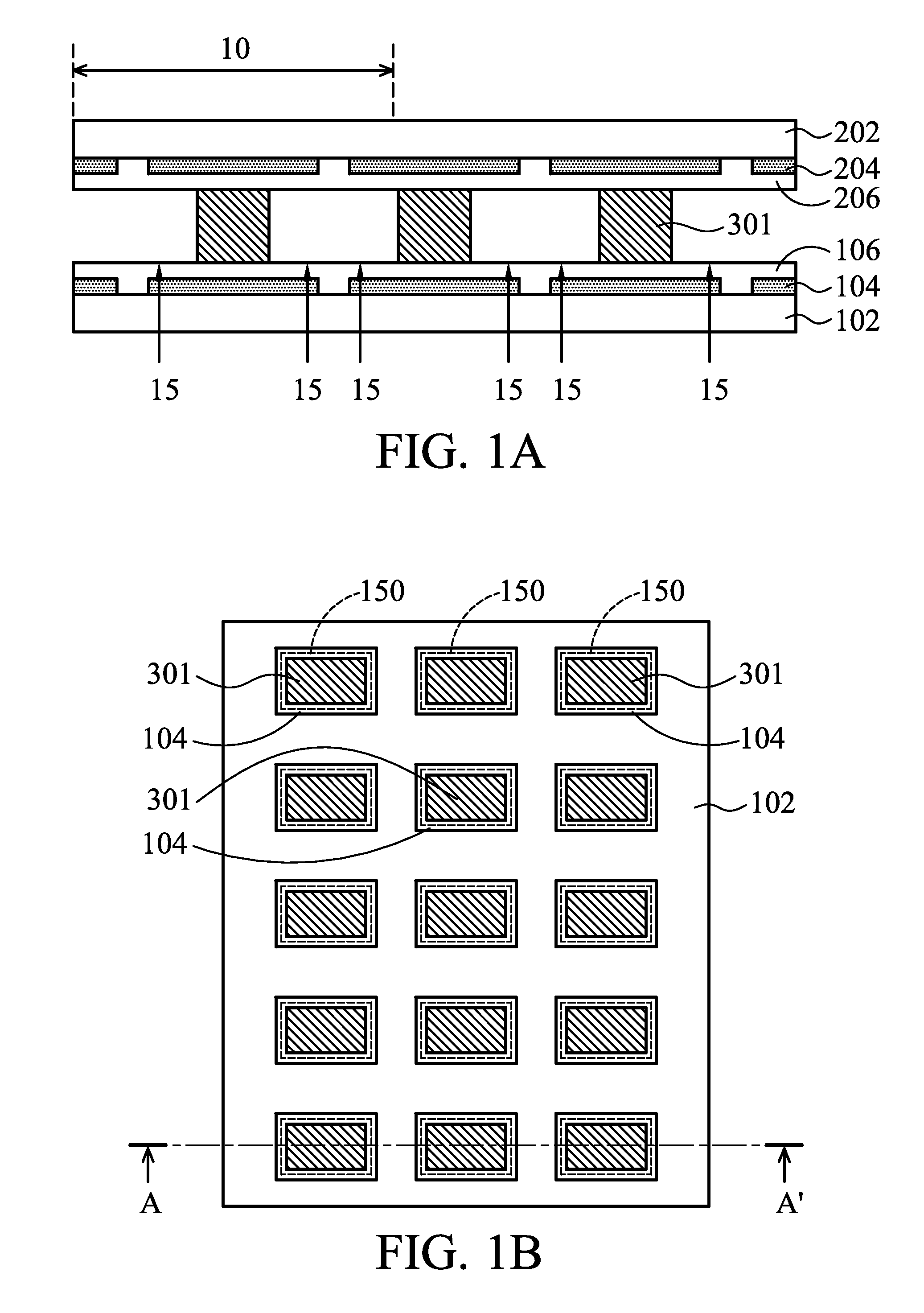
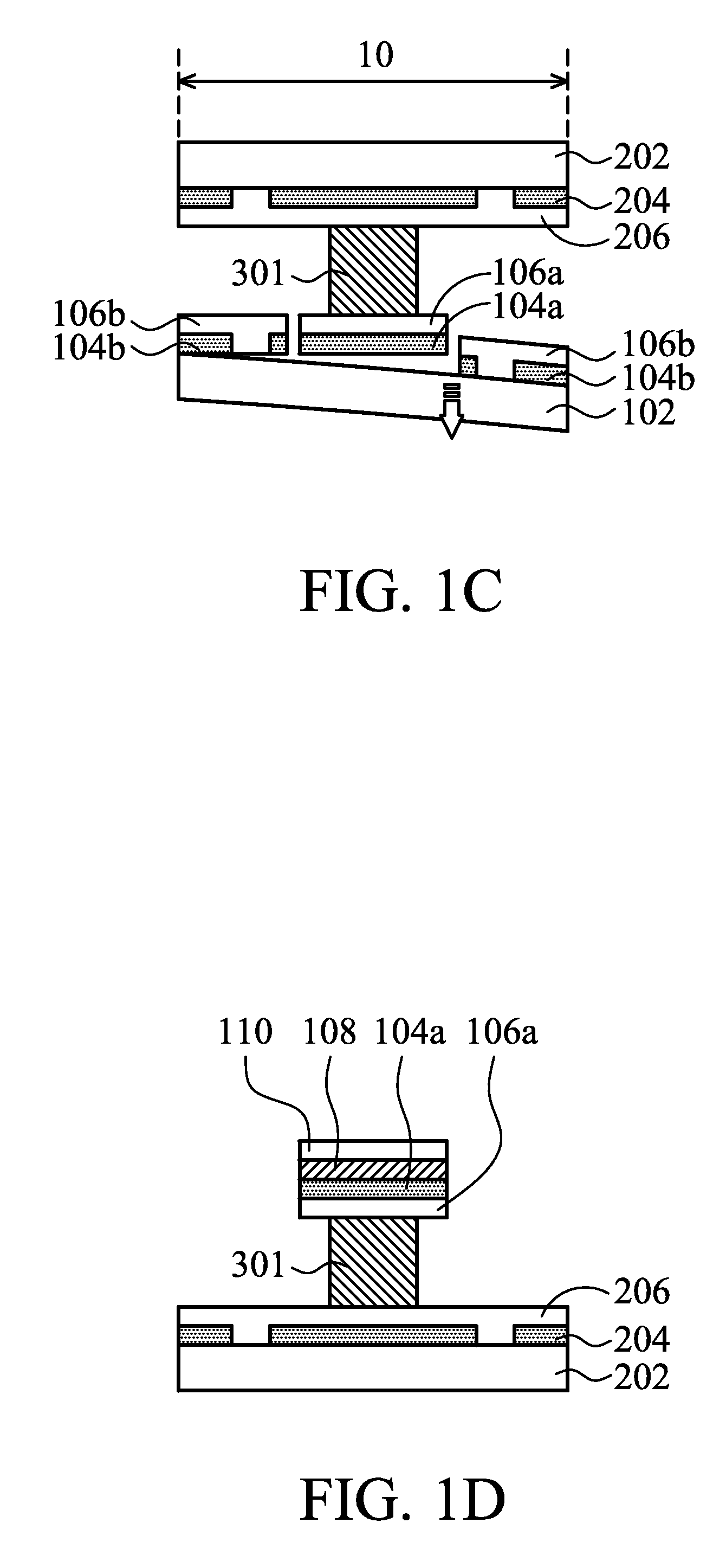
[0025]FIGS. 1A and 1C-1F show cross-sectional schematic representations of various stages of fabricating a flexible electronic device in accordance with the disclosure. Referring to FIG. 1A, a first rigid carrier substrate 102 and a second rigid carrier substrate 202 are disposed oppositely to each other. A plurality of first de-bonding areas 104, a first flexible substrate 106, at least one flexible electronic device 301, a second flexible substrate 206, a plurality of second de-bonding areas 204 and the second rigid carrier substrate 202 are formed on the first rigid carrier substrate 102. The flexible electronic device 301 may be a single flexible electronic device or many flexible electronic devices. The flexible electronic device 301 is formed between the first rigid carrier substrate 102 and the second rigid carrier substrate 202, and between the first flexible substrate 106 and the second flexible substrate 206. The first de-bonding areas 104 and second de-bonding areas 204 a...

second embodiment

[0054]In a modified embodiment of the second embodiment, one of the first rigid carrier substrate 102 and the second rigid carrier substrate 202 is a transparent substrate, and the other is a non-transparent substrate, such as metal substrate, or stainless steel substrate. When one of the two rigid carrier substrates is a transparent substrate, and the other is a non-transparent substrate, note that the cutting step is performed from the transparent substrate side.

third embodiment

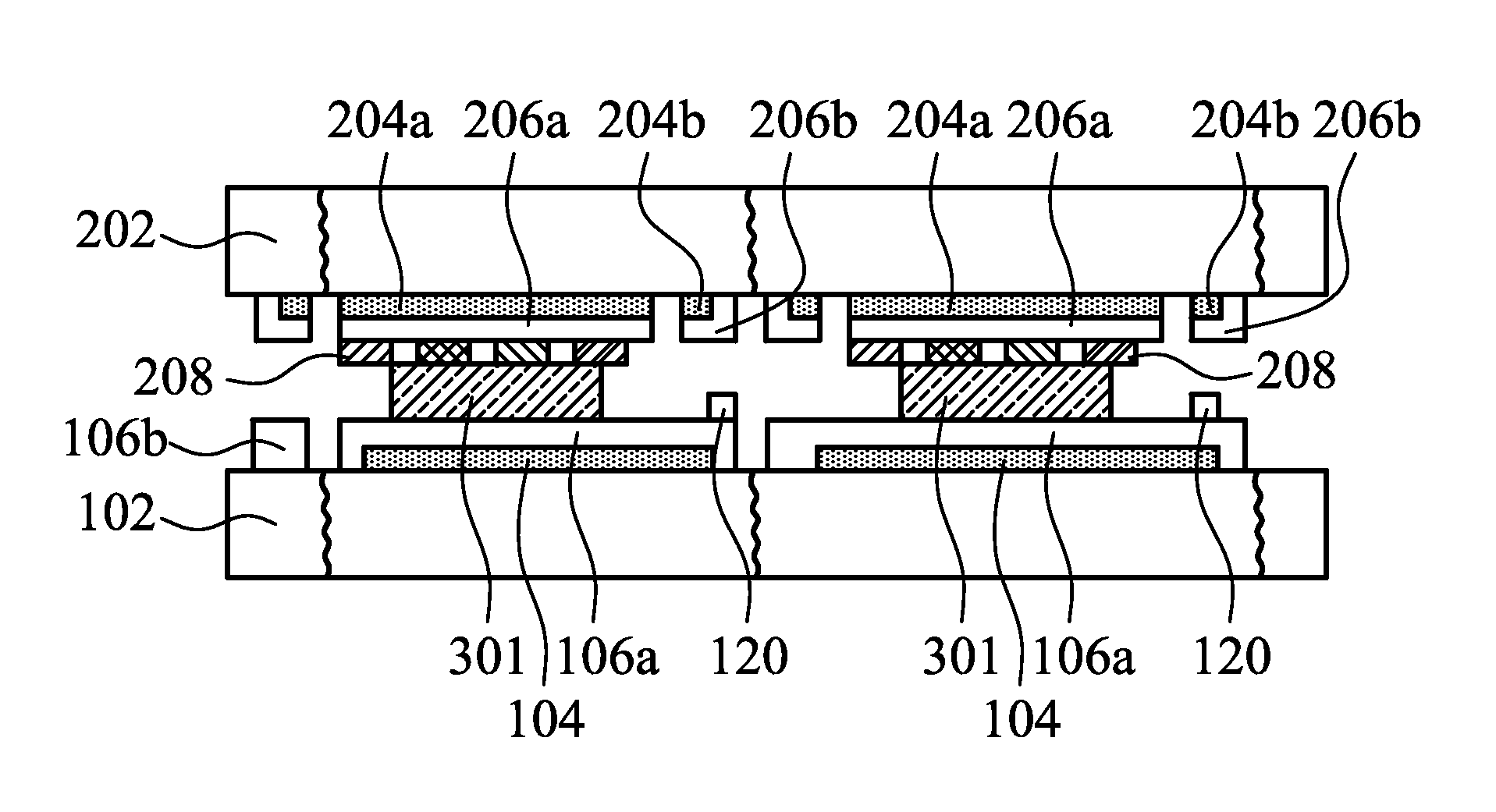
[0055]FIGS. 3A-3D show cross-sectional schematic representations of various stages of fabricating a flexible electronic device in accordance with the disclosure, wherein like elements are identified by the same reference numbers as in FIG. 1A-1F, and thus omitted for brevity.

[0056]Referring to FIG. 3A, a cutting step 15 is performed to cut through the first de-bonding areas 104, a first flexible substrate 106, the second de-bonding areas 204 and the second flexible substrate 206. The first de-bonding areas 104 are divided into a first portion 104a and a second portion 104b, the first flexible substrate 106 is divided into a first portion 106a and a second portion 106b, the second de-bonding areas 204 are divided into a third portion 204a and a fourth portion 204b, and the second flexible substrate 206 is divided into a third portion 206a and a fourth portion 206b. The flexible electronic device 301 is formed on the first portion 104a of the first de-bonding areas 104 and the first p...


PUM


Abstract

The disclosure provides a method for fabricating the flexible electronic devices, including: providing a first rigid carrier substrate and a second rigid carrier substrate, wherein at least one flexible electronic device is formed between the first rigid carrier substrate and the second rigid carrier substrate, and a plurality of first de-bonding areas, a first flexible substrate, the flexible electronic device, a second flexible substrate, a plurality of second de-bonding areas and the second rigid carrier substrate are formed on the first rigid carrier substrate; performing a first cutting step to cut through the first de-bonding areas; separating the first rigid carrier substrate from the first de-bonding areas; removing the first rigid carrier substrate from the first de-bonding areas; and performing a second cutting step to cut through the second de-bonding areas; separating and removing the second rigid carrier substrate from the second de-bonding areas.

Description

CROSS REFERENCE TO RELATED APPLICATION[0001]This Application claims priority of Taiwan Patent Application No. 100123479, filed on Jul. 4, 2011, and No. 100147906, filed on Dec. 22, 2011, the entirety of which is incorporated by reference herein.BACKGROUND OF THE DISCLOSURE[0002]1. Field of the Disclosure[0003]The disclosure relates to a method for fabricating the electronic devices.[0004]2. Description of the Related Art[0005]Consumer electronic applications are becoming increasingly diverse with the rapid progress of science and technology. Light, thin, short and small electronic products are being demanded. Thus, flexible electronic devices are being developed.[0006]During fabrication of the flexible electronic devices, the flexible electronic devices are firstly formed on a flexible substrate with a glass rigid carrier substrate. Then, the flexible electronic devices are taken out of the rigid carrier substrate.[0007]U.S. Pat. No. 7,466,390 discloses a method for fabricating a th...

Claims


Application Information

Patent Timeline
Patent Type & Authority Applications(United States)
IPC IPC(8): H01L21/78
CPCH01L51/003H01L51/0097H01L2251/566H01L2251/5338H01L2227/326H10K71/80H10K77/111H10K59/1201H10K2102/311H10K71/851
Inventor CHEN, KUANG-JUNGCHAN, ISAAC WING-TAK
Owner HANNSTAR DISPLAY CORPORATION
Why Eureka
Try Eureka