Structure and process of heat dissipation substrate

a heat dissipation substrate and heat dissipation technology, applied in the field of metal substrates, can solve the problems of easy bend and deformation of the heat dissipation substrate, inconvenient operation, and insufficient steps and fabrication costs, and achieve the effect of reducing fabrication steps and fabrication costs

US20130043016A1Inactive Publication Date: 2013-02-21SUBTRON TECH
5 Cites 0 Cited by

Patent Information

Authority / Receiving Office
US · United States
Patent Type
Applications(United States)
Current Assignee / Owner
Publication Date
2013-02-21
Estimated Expiration
Not applicable · inactive patent

Smart Images

  • Figure 1
    Figure 1
  • Figure 2
    Figure 2
  • Figure 3
    Figure 3
Patent Text Reader

Abstract

Structure of a heat dissipation substrate including a metal substrate, a first insulating material, a second insulating material, a first patterned conductive layer and a second patterned conductive layer is provided. The metal substrate has an upper surface and a lower surface opposite to each other, a plurality of first recesses located on the upper surface and a plurality of second recesses located on the lower surface. The first insulating material is provided to fill into the first recesses. The second insulating material is provided to fill into the second recesses. The first patterned conductive layer is disposed on the upper surface of the metal substrate and a portion of the first insulating material. The second patterned conductive layer is disposed on the lower surface of the metal substrate and a portion of the second insulating material.
Need to check novelty before this filing date? Find Prior Art

Description

CROSS-REFERENCE TO RELATED APPLICATION

[0001] This application claims the priority benefit of Taiwan application serial no. 100129781, filed on Aug. 19, 2011. The entirety of the above-mentioned patent application is hereby incorporated by reference herein and made a part of this specification.BACKGROUND OF THE INVENTION

[0002] 1. Field of the Invention

[0003] The invention relates to a metal substrate, more particularly, the invention relates to a structure of a heat dissipation substrate adopted in a heating device and a fabricating process of the same.

[0004] 2. Description of Related Art

[0005] With the progression in fabricating technology, light emitting diodes (LEDs) have gradually increased the light emitting efficiency through persistent research and improvement to further enhance the light emitting brightness thereof so as to satisfy demands in various products. In other words, other than improving the external packaging thereof, LEDs also require advanced design to achieve higher e...

Examples

Embodiment Construction

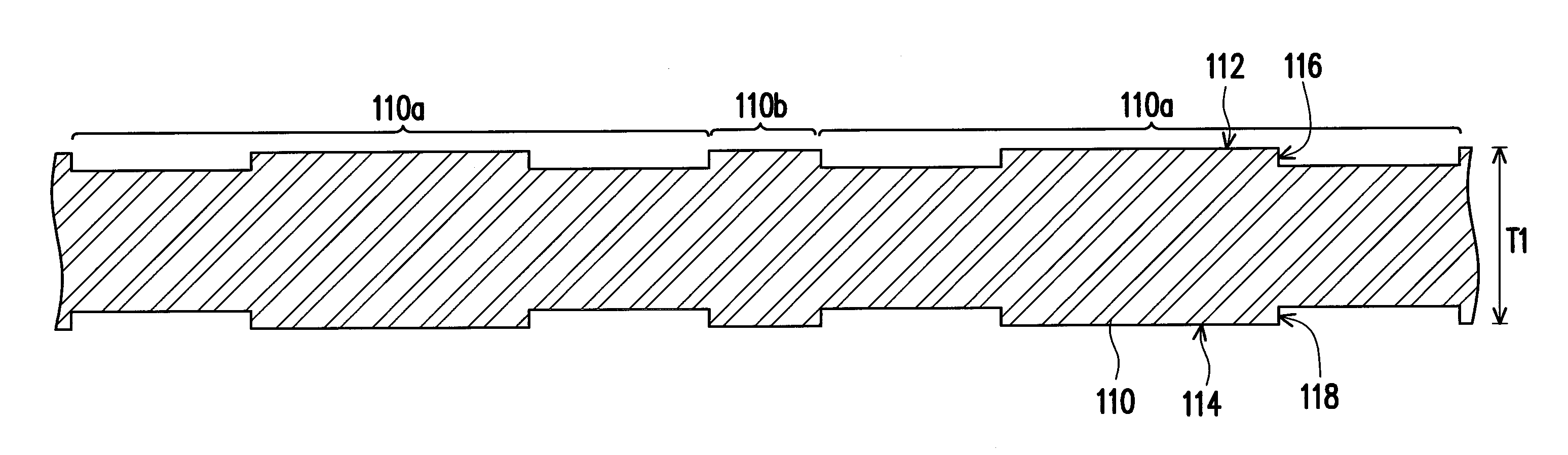
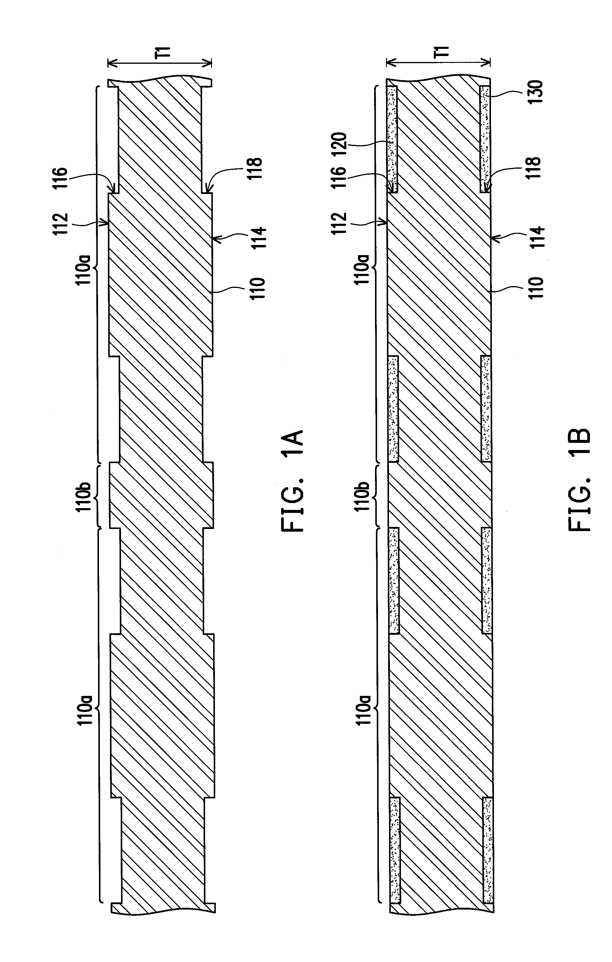
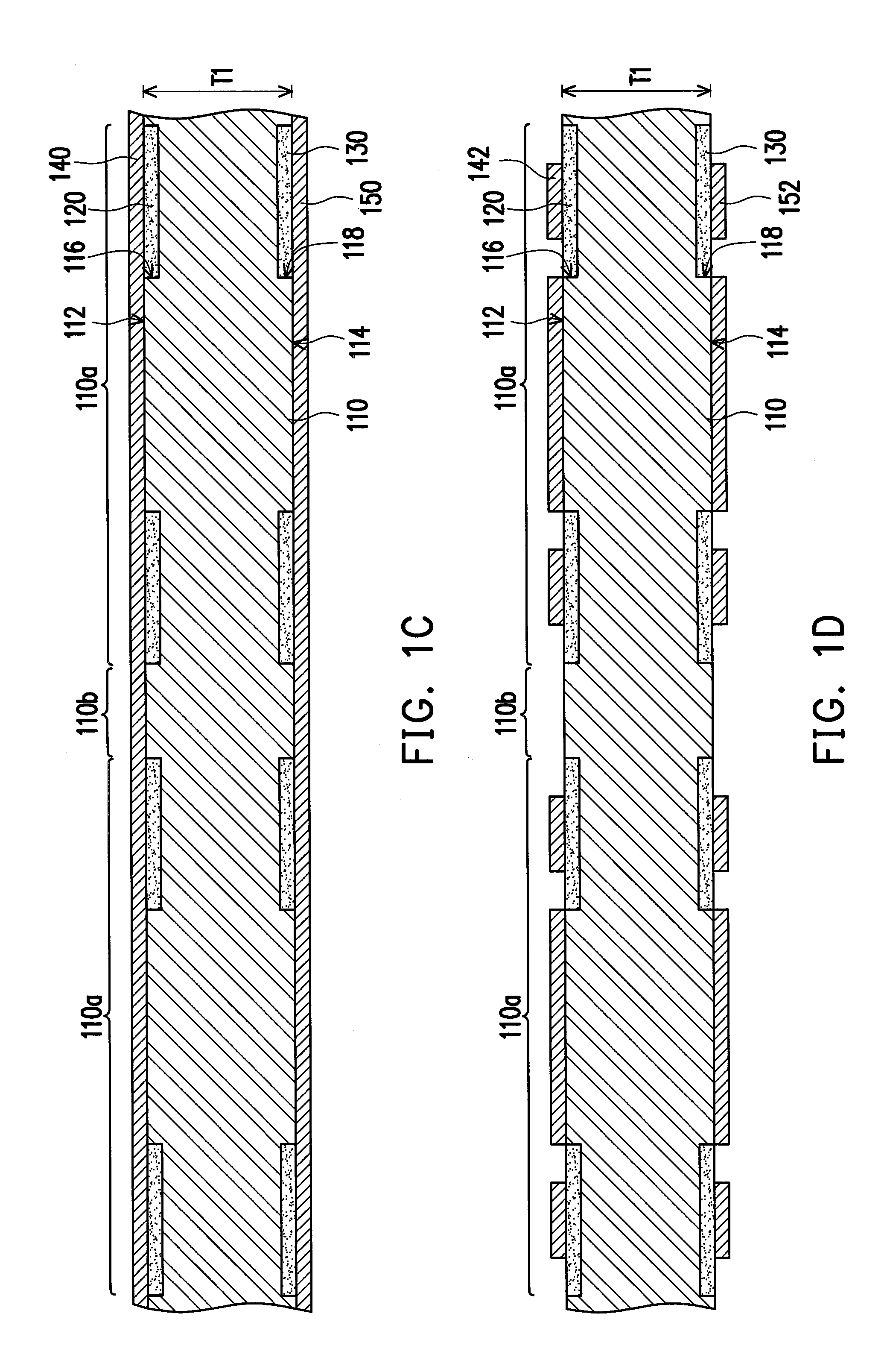
[0023]FIGS. 1A to 1E are schematic cross-sectional views illustrating a flowchart of a fabrication process of a heat dissipation substrate in one embodiment of the invention. FIG. 1F is a schematic cross-sectional view of a heating device loaded on a heat dissipation substrate in FIG. 1E. Referring to FIG. 1A, according to a method of fabricating a heat dissipation substrate of the present embodiment, a metal substrate 110 is first provided. The metal substrate 110 has an upper surface 112 and a lower surface 114 opposite to each other. The metal substrate 110 has a thickness T1 less than 0.6 millimeter (mm) and is fabricated with copper, for example.

[0024]Referring to FIG. 1A, a plurality of first recesses 116 is formed on the upper surface 112 of the metal substrate 110 and a plurality of second recesses 118 is formed on the lower surface 114 of the metal substrate 110. Here, positions of the first recesses 116 correspond to positions of the second recesses 118 respectively. In th...