Package structure and fabrication method thereof

Active Publication Date: 2015-06-11
SILICONWARE PRECISION IND CO LTD
View PDF3 Cites 14 Cited by
  • Summary
  • Abstract
  • Description
  • Claims
  • Application Information

AI Technical Summary

Benefits of technology

The present invention eliminates the need for through holes in silicon substrates, reducing equipment and fabrication costs. It also integrates two types of sensors in a SiP package, resulting in low power consumption, low cost, and high performance. The package structure is also smaller, meeting the miniaturization requirement.

Problems solved by technology

However, such a package structure has a large size, which fails to meet the miniaturization requirement of end products.
However, the TSV technique is costly and requires a high degree of accuracy, thereby complicating the fabrication process and increasing the fabrication cost.

Method used


Image

  • Package structure and fabrication method thereof
  • Package structure and fabrication method thereof
  • Package structure and fabrication method thereof

Examples


first embodiment

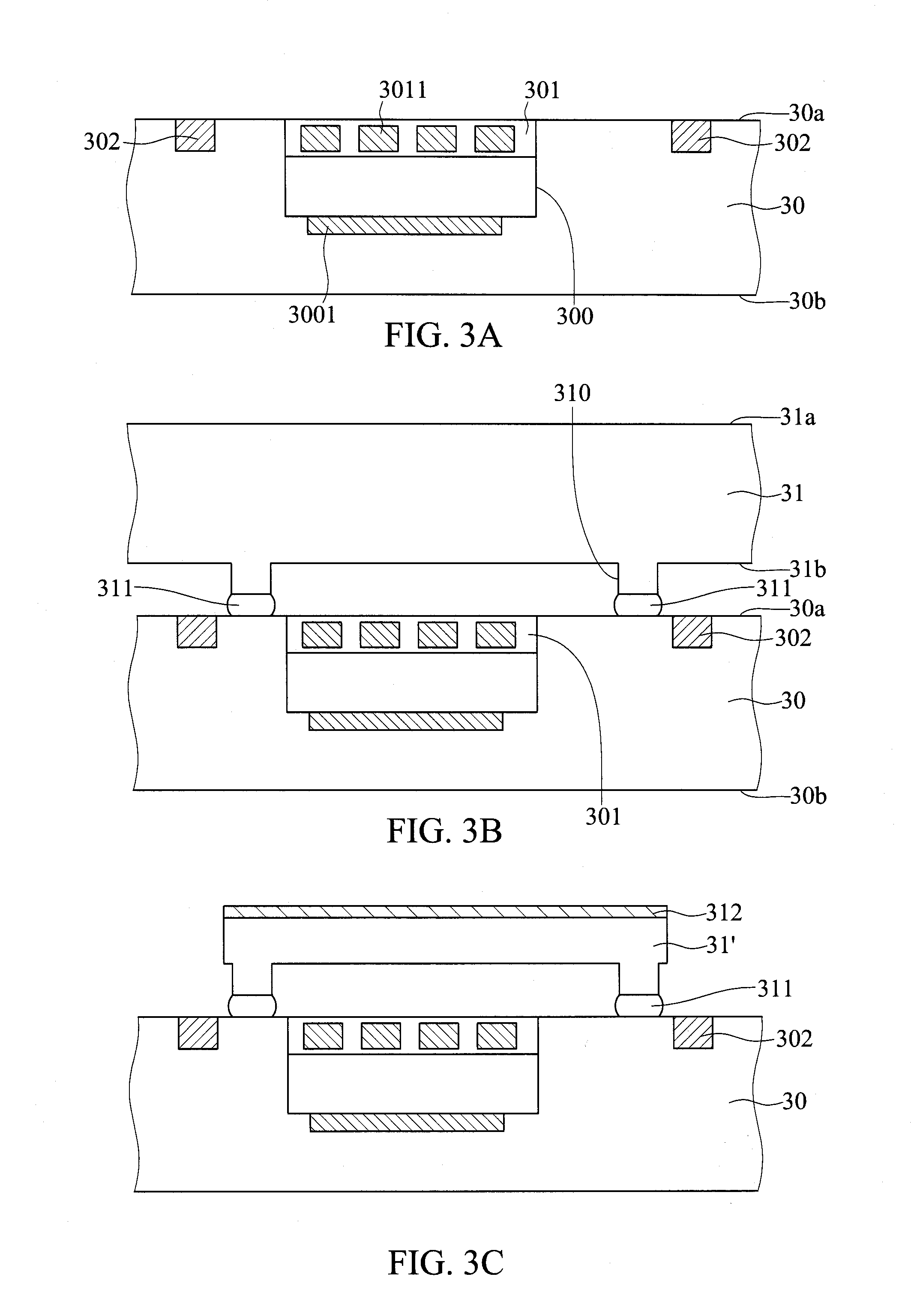
[0029]FIGS. 3A to 3J are schematic cross-sectional views showing a package structure and a fabrication method thereof according to a first embodiment of the present invention.

[0030]Referring to FIG. 3A, a first wafer 30 having opposite first and second surfaces 30a, 30b is provided. The first surface 30a of the first wafer 30 has a groove 300, a thin film 301 closing an open end of the groove 300, and a plurality of electrical contacts 302. A plurality of upper electrodes 3011 are formed in the thin film 301 and a plurality of lower electrodes 3001 are formed on a bottom of the groove 300. The first wafer 30 can be a pressure or temperature sensor wafer having a MEMS element. The closed groove 300 is in a vacuum state.

[0031]Referring to FIG. 3B, a second wafer 31 is disposed on the first wafer 30. The second wafer 31 has opposite third and fourth surfaces 31a, 31b, and the fourth surface 31b of the second wafer 31 has a concave portion 310 and a seal ring 311 located at a periphery ...

second embodiment

[0040]FIGS. 4A to 41 are schematic cross-sectional views showing a package structure and a fabrication method thereof according to a second embodiment of the present invention.

[0041]Referring to FIG. 4A, a first wafer 30 having opposite first and second surfaces 30a, 30b is provided. The first surface 30a of the first wafer 30 has a groove 300, a thin film 301 closing an open end of the groove 300, and a plurality of electrical contacts 302. A plurality of upper electrodes 3011 are formed in the thin film 301 and a plurality of lower electrodes 3001 are formed on a bottom of the groove 300. The first wafer 30 can be a pressure or temperature sensor wafer having a MEMS element. The closed groove 300 is in a vacuum state.

[0042]Referring to FIG. 4B, a chip 41 is disposed on the first wafer 30. The chip 41 can be a motion sensor. The chip 41 has a third surface 41a with a plurality of electrode pads 411 and an opposite fourth surface 41b with a concave portion 410 and a seal ring 412 lo...


PUM


Abstract

A package structure is provided, which includes: a wafer having a surface with a groove, a thin film closing an open end of the groove and electrical contacts; a chip having a surface with a conductive layer and an opposite surface with a concave portion and a seal ring located at a periphery of the concave portion, the chip being disposed on the wafer with the seal ring surrounding the thin film and the electrical contacts located outside the seal ring; an encapsulant formed on the wafer for encapsulating the chip and the electrical contacts; a plurality of sub-conductive wires embedded in the encapsulant with one ends exposed from a top surface of the encapsulant and the other ends in electrical connection with the electrical contacts; and a through hole penetrating the wafer and communicating with the concave portion, thereby reducing the fabrication cost and size of the package structure.

Description

BACKGROUND OF THE INVENTION[0001]1. Field of the Invention[0002]The present invention relates to package structures and fabrication methods thereof, and more particularly, to a package structure having a MEMS (Micro-Electro-Mechanical System) element and a fabrication method thereof.[0003]2. Description of Related Art[0004]MEMS elements have integrated electrical and mechanical functions and can be fabricated through various micro-fabrication technologies. A MEMS element is generally disposed on a substrate and protected by a cover or an encapsulant from being damaged by external environment.[0005]FIG. 1 is a schematic cross-sectional view of a conventional package structure having a MEMS element. Referring to FIG. 1, a MEMS element 11, such as a pressure sensing element, is disposed on an LGA (Land Grid Array) substrate 10, and electrical contacts 111 of the MEMS element 11 are electrically connected to electrical contacts 101 of the LGA substrate 10 by wire bonding. Then, a metal ...

Claims


Application Information

Patent Timeline
IPC IPC(8): H01L23/48G01K13/00G01L1/00H01L21/768H01L23/28
CPCH01L23/481H01L21/768G01K13/00G01L1/00H01L23/28H01L23/10H01L2224/48091B81B7/0061B81B7/007B81B2207/098G01L19/0076G01L19/147H01L2924/00014
Inventor CHANG, HONG-DACHIU, SHIH-KUANG
Owner SILICONWARE PRECISION IND CO LTD
Why Eureka
Try Eureka