
Sensor-type semiconductor package and fabrication method thereof

a technology of semiconductor packages and fabrication methods, applied in semiconductor devices, semiconductor/solid-state device details, electrical apparatus, etc., can solve the problems of difficult control of the clamping force between the protruding portion and the substrate, contamination of the area for mounting chips and bonding wires, and damage to the substrate, so as to reduce the manufacturing cost and reduce the process reliability. , the effect of eliminating the clamping pressur

Inactive Publication Date: 2008-05-08
SILICONWARE PRECISION IND CO LTD
View PDF9 Cites 5 Cited by
  • Summary
  • Abstract
  • Description
  • Claims
  • Application Information

AI Technical Summary

Benefits of technology

[0011]According to the above drawbacks, an objective of the present invention is to provide a lighter, thinner, shorter and smaller sensor-type semiconductor package without a dam lattice and a fabrication method thereof.
[0012]Another objective of the present invention is to provide a sensor-type semiconductor package, which is encapsulated by an encapsulant and has a high reliability, and a fabrication method thereof.
[0013]Still another objective of the present invention is to provide a low cost sensor-type semiconductor package and a fabrication method thereof.
[0014]A further objective of the present invention is to provide a sensor-type semiconductor package free from damaging the glass and sensor chip and a fabrication method thereof.
[0020]As the dam lattice is not employed in the present invention, the sensor-type semiconductor package obtained according to the present invention becomes much thinner and smaller, the process reliability is increased and the fabrication cost is decreased. Meanwhile, as a covering layer is preformed on the light-permeable body and the encapsulant is formed on the covering layer during the molding process, the mold clamping pressure can be eliminated from being directly stressed on the light-permeable body as in the prior art, thereby preventing cracking of the light-permeable body and the sensor chip below the light-permeable body. In addition, the covering layer can protect the light-permeable body from being contaminated by the overflow during the molding process. Furthermore, the conventional molding process employed in the present invention can reduce fabrication cost and facilitate batch-type fabrication of semiconductor packages, thus reducing the fabrication cost and process complexity.

Problems solved by technology

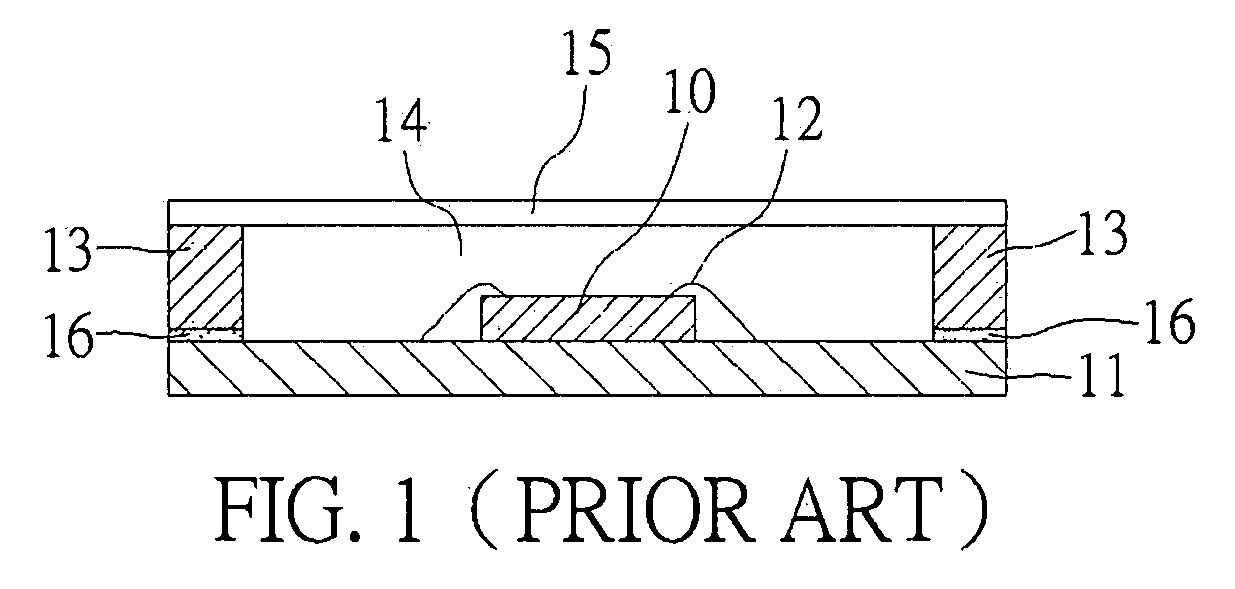
However, the above-described semiconductor package has several drawbacks.
For example, the clamping force between the protruding portion and the substrate is difficult to control.
If the protruding portion cannot be stably contacted with the substrate, the resin compound can easily overflow to the area between the protruding portion and the substrate, thereby causing contamination of the areas for mounting chip and bonding wires.
On the other hand, if the protruding portion is tightly pressed against the substrate, the substrate can be damaged.
Further, the fabrication cost for the mold having the protruding portion is high, and the mold needs to be changed according to different size of the predefined area of the substrate, thereby greatly increasing the fabrication cost and fabrication complexity.
However, a common problem exists in the above-described techniques.
That is, as spaces need to be reserved for the dam lattice in the above-described semiconductor packages, it limits the packages size being further miniaturized.
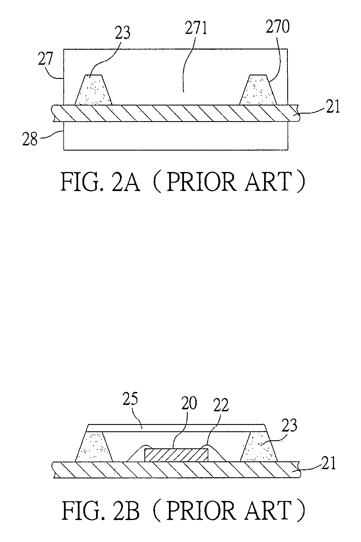
However, such a method has high fabrication cost and poor product reliability, thus limiting its application in the industry.
However, because the glass 45 is directly abutted against the top of the upper mold, the upper and low mold clamping pressure is directly stressed on the glass 45, which can cause cracking of the glass 45 and further damage the sensor chip 40 below the glass 45.
In addition, if a gap is existed between the upper mold and the glass, overflow of encapsulant can occur and thus surface of the glass 45 is contaminated.

Method used


Image

  • Sensor-type semiconductor package and fabrication method thereof
  • Sensor-type semiconductor package and fabrication method thereof
  • Sensor-type semiconductor package and fabrication method thereof

Examples


first embodiment

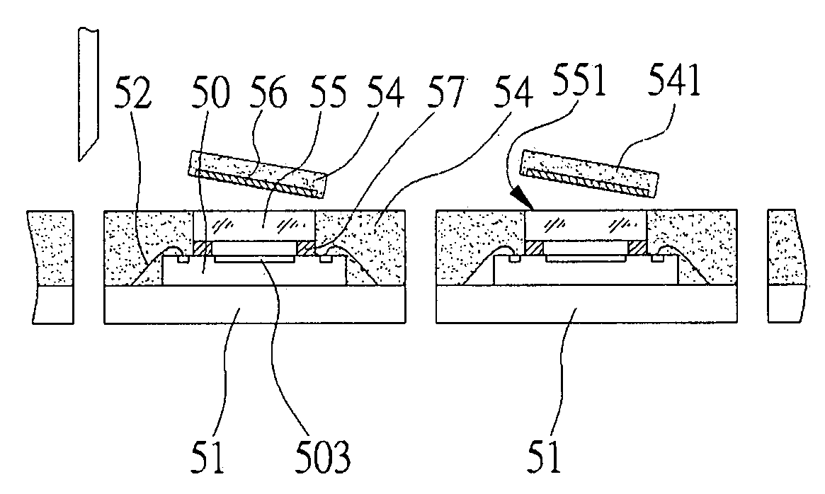
[0030]FIGS. 5A to 5F are schematic cross-sectional diagrams showing a fabrication method of a sensor-type semiconductor package according to a first embodiment of the present invention. In the present embodiment, the sensor-type semiconductor package is fabricated in batch-type.

[0031]As shown in FIGS. 5A and 5B, a wafer 50A having a plurality of sensor chips 50 is provided, and a plurality of light-permeable bodies 55 are respectively attached to the sensor chips 50. Each light-permeable body has a first surface 551 and a second surface 552 opposing to the first surface 551. A covering layer 56 is formed on the first surface 551 and a ring-shaped adhesive layer 57 is formed on the second surface 552. The light-permeable bodies 55 are attached to the sensor chips 50 through the ring-shaped adhesive layers 57. In addition, a planar size of each of the light-permeable bodies 55 is smaller than that of each of the sensor chips 50. The wafer 50A is then singulated so as to obtain a plura...

second embodiment

[0040]FIGS. 6A to 6E are schematic cross-sectional diagrams showing a fabrication method of a sensor-type semiconductor package according to a second embodiment of the present invention. The main difference of the present embodiment from the first embodiment is that the sensor chips are attached to and electrically connected with the substrates before the light-permeable bodies with the covering layers and the adhesive layers from thereon are attached to the sensor chips.

[0041]As shown in FIG. 6A, a substrate module 61A having a plurality of substrates 61 is provided, and sensor chips 60 are attached to the substrates 61. Each sensor chip 60 has an active surface 601 and a non-active surface 602 opposing to the active surface 601, and a sensor area 603 and bonding pads 604 are disposed on the active surface 601. The sensor chips 60 are attached to the substrates 61 through the non-active surfaces 602 thereof, and the bonding pads 604 of the sensor chips 60 are electrically connected...

third embodiment

[0046]FIG. 7 is a schematic cross-sectional diagram showing a fabrication method of a sensor-type semiconductor package according to a third embodiment of the present invention. In the present embodiment, for facilitating the removal of the covering layer 76 and the encapsulant 74 located on the covering layer 76, a protruding portion 741 is formed on the top surface of the encapsulant 74. Thus, a clamping tool 78 can be employed to clamp the protruding portion 741 for removing the covering layer 76 and the encapsulant 74 located on the covering layer 76.

[0047]Therefore, the present invention mainly comprises attaching a plurality of light-permeable bodies each having a covering layer and an adhesive layer to a wafer having a plurality of sensor chips, wherein a planar size of each of the light-permeable bodies is smaller than that of each of the sensor chips; singulating the wafer so as obtain a plurality of separated sensor chips with the light-permeable bodies attached thereon; a...


PUM


Abstract

A sensor-type semiconductor package and a fabrication method thereof are provided. The fabrication method of the sensor-type semiconductor package includes steps of: providing a wafer having sensor chips; attaching light-permeable bodies to the sensor chips, wherein each light-permeable body has a covering layer and an adhesive layer; singulating the wafer so as to obtain a plurality of separated sensor chips with the light-permeable bodies attached thereon; attaching and electrically connecting the separated sensor chips to a substrate module having substrates, forming an encapsulant encapsulating the sensor chips and the light-permeable bodies; cutting the encapsulant along edges of the light-permeable bodies to a depth at least corresponding the bottom edges of the covering layers; removing the covering layers with the encapsulant mounted thereon to expose the light-permeable bodies; and cutting between the substrates to obtain a plurality of sensor-type semiconductor packages.

Description

FIELD OF THE INVENTION[0001]The present invention relates generally to semiconductor packages and fabrication methods thereof, and more particularly to sensor-type semiconductor packages and fabrication methods thereof.BACKGROUND OF THE INVENTION[0002]Conventionally, to obtain an image sensor package, a sensor chip is mounted to a chip carrier and electrically connected to the chip carrier via the bonding wires, then the top surface of the sensor chip is covered by a glass such that image light can be captured by the sensor chip. Thereafter, such an image sensor-type package is integrated to an external device such as a printed circuit board for further being applied in various kinds of electronic products such as digital cameras, digital videos, optical mouse, mobile phones and so on.[0003]Referring to FIG. 1, a sensor-type semiconductor package disclosed by U.S. Pat. No. 6,060,340 is shown. A dam lattice 13 is prepared and attached to a substrate 11 by an adhesive 16. The dam latt...

Claims


Application Information

Patent Timeline
Patent Type & Authority Applications(United States)
IPC IPC(8): H01L31/0203H01L31/18
CPCH01L23/3128H01L27/14618H01L2924/16195H01L31/0203H01L2224/48247H01L27/14683H01L2924/181H01L24/97H01L2924/16235H01L2924/00012
Inventor HUANG, CHIEN-PINGCHANG, TSE-WENCHAN, CHANG-YUEHCHANG, CHENG-YI
Owner SILICONWARE PRECISION IND CO LTD
Learn More