
Memory command scheduler and memory command scheduling method
- Summary
- Abstract
- Description
- Claims
- Application Information
AI Technical Summary
Benefits of technology
Problems solved by technology
Method used
Image

Examples
Embodiment Construction
[0050]Hereinafter, various exemplary embodiments will be described in detail with reference to the accompanying drawings.
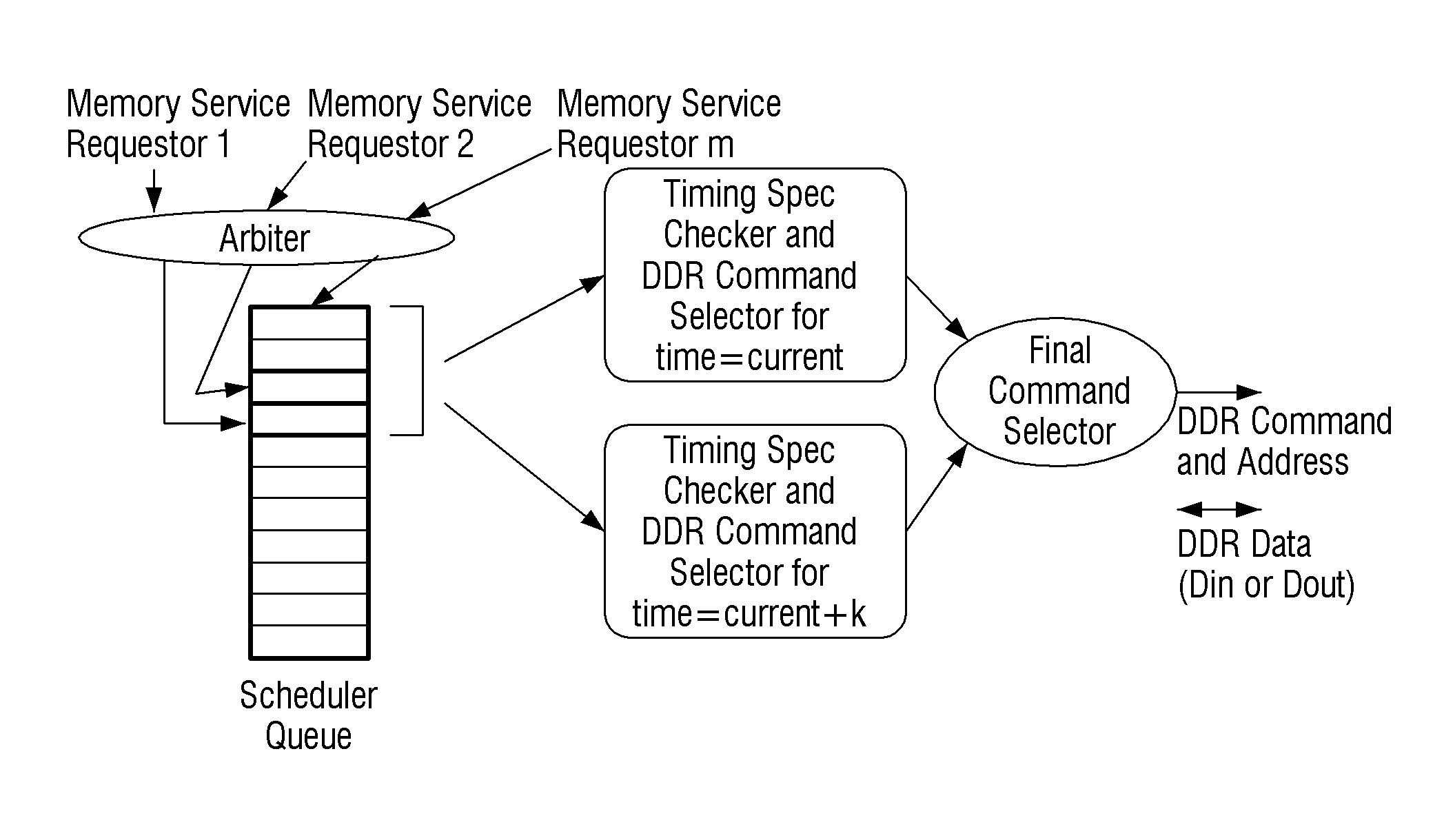
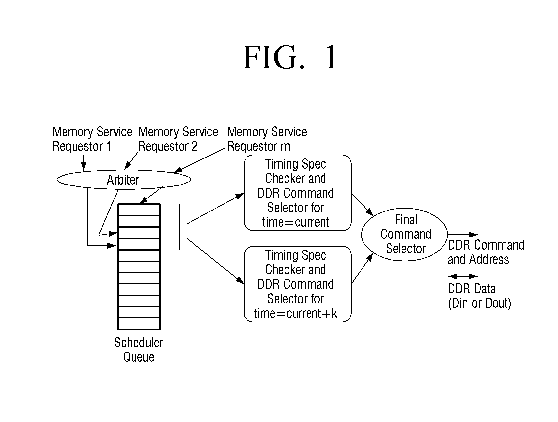
[0051]FIG. 1 is a diagram of an external interface and a memory command scheduler structure.
[0052]It is assumed that an m external devices may make a memory read or write request (where, m indicates an integer), and an arbitrating apparatus in a simple round robin or at least recently used scheme may be used. Even though a request for different data sizes is received, the requested data size is converted into a block unit. One block includes a plurality of bytes sent to a target DDRx SDRAM chip through a data bus interface within 8 bursts (4 clock cycles). Two entries are selected in a scheduler queue during each clock cycle. A first entry, which corresponds to an entry to be currently executed, is determined based on a current bank state, a parameter for the entry, and a latency time interval limit between several DDR commands specified in a DDRx specification.
[0...
PUM
 Abstract
Description
Claims
Application Information