Multi port processor architecture

a processor and multi-port technology, applied in the direction of electric digital data processing, instruments, etc., can solve the problems of processor centric and unbalanced prior art systems, bus latency can be problematic, and latency can be even more problematic, so as to reduce memory access latency, avoid bus latencies, and reduce latency

Inactive Publication Date: 2006-05-11
TOSHIBA AMERICA ELECTRONICS COMPONENTS
View PDF11 Cites 2 Cited by
  • Summary
  • Abstract
  • Description
  • Claims
  • Application Information

AI Technical Summary

Benefits of technology

[0011] In accordance with an aspect of the present invention, memory access latency can be reduced by using a dedicated channel to access the memory system. The present invention can be used with any memory interface. By using an open interface standard, such as Open Core Protocol (OCP), the present invention can be implemented without using new memory commands. The present invention can provide predictable memory access delays for a dedicated device, such as a processor and reduced latency by using priority handling and avoids bus latencies. The predictable low latency architectural approach of the present invention can reduces memory latency, and can reduce memory latency to less than thirty clock cycles, while not reducing memory bandwidth efficiency.

Problems solved by technology

Traditionally, prior art systems tend to be processor centric and not balanced.
Because the CPU, memory, and peripherals (when accessing memory) share the same bus, bus latency can be problematic.
This latency can be even more problematic in hierarchical bus systems.
However, the bus arbiter adds to the overhead in accessing the bus and can cause even more latency.
However, these approaches are expensive.
Furthermore, these approaches can introduce other problems, e.g. increasing the clock speed (frequency) of the system bus requires more power and generates additional heat.

Method used


Image

  • Multi port processor architecture
  • Multi port processor architecture
  • Multi port processor architecture

Examples


Embodiment Construction

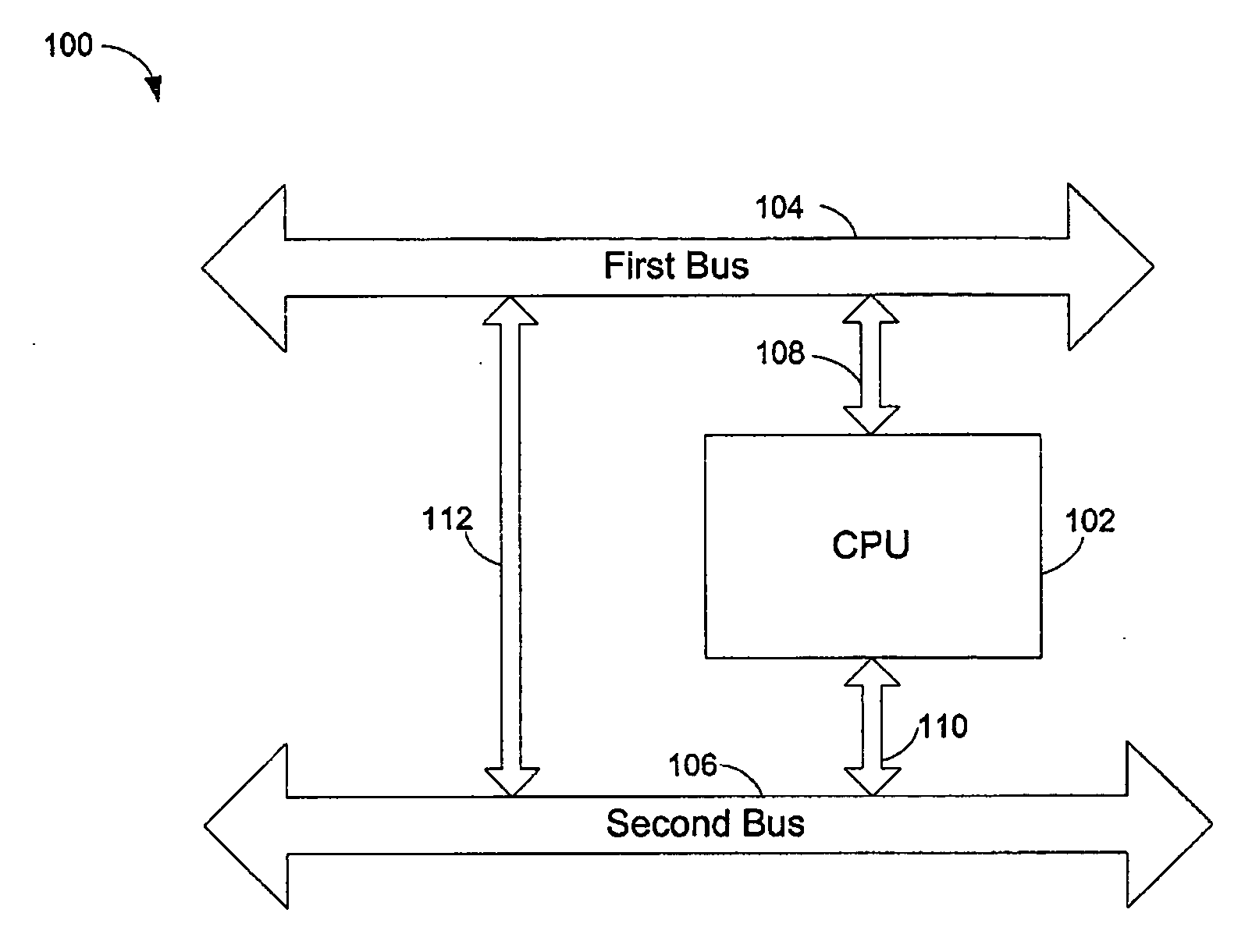
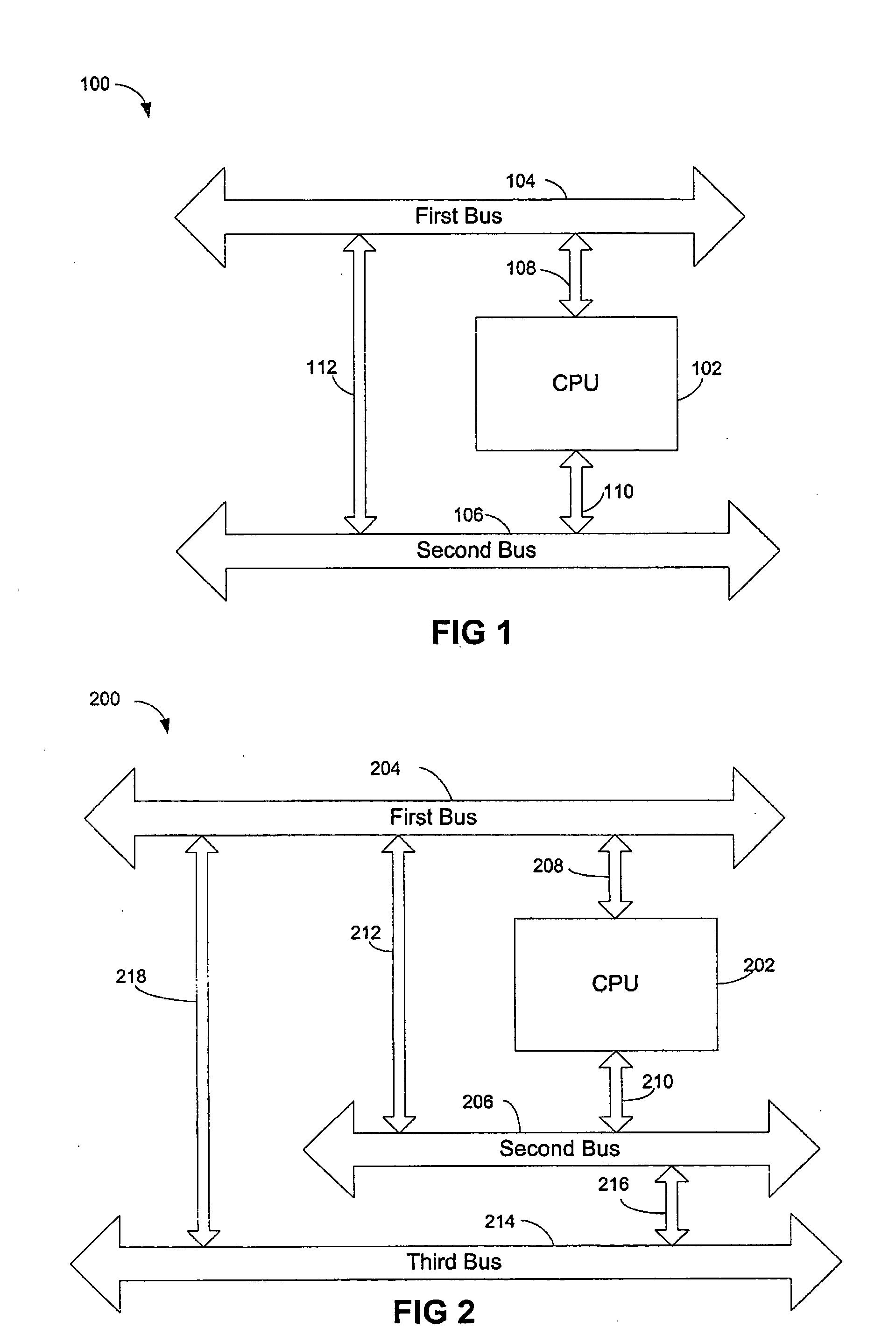
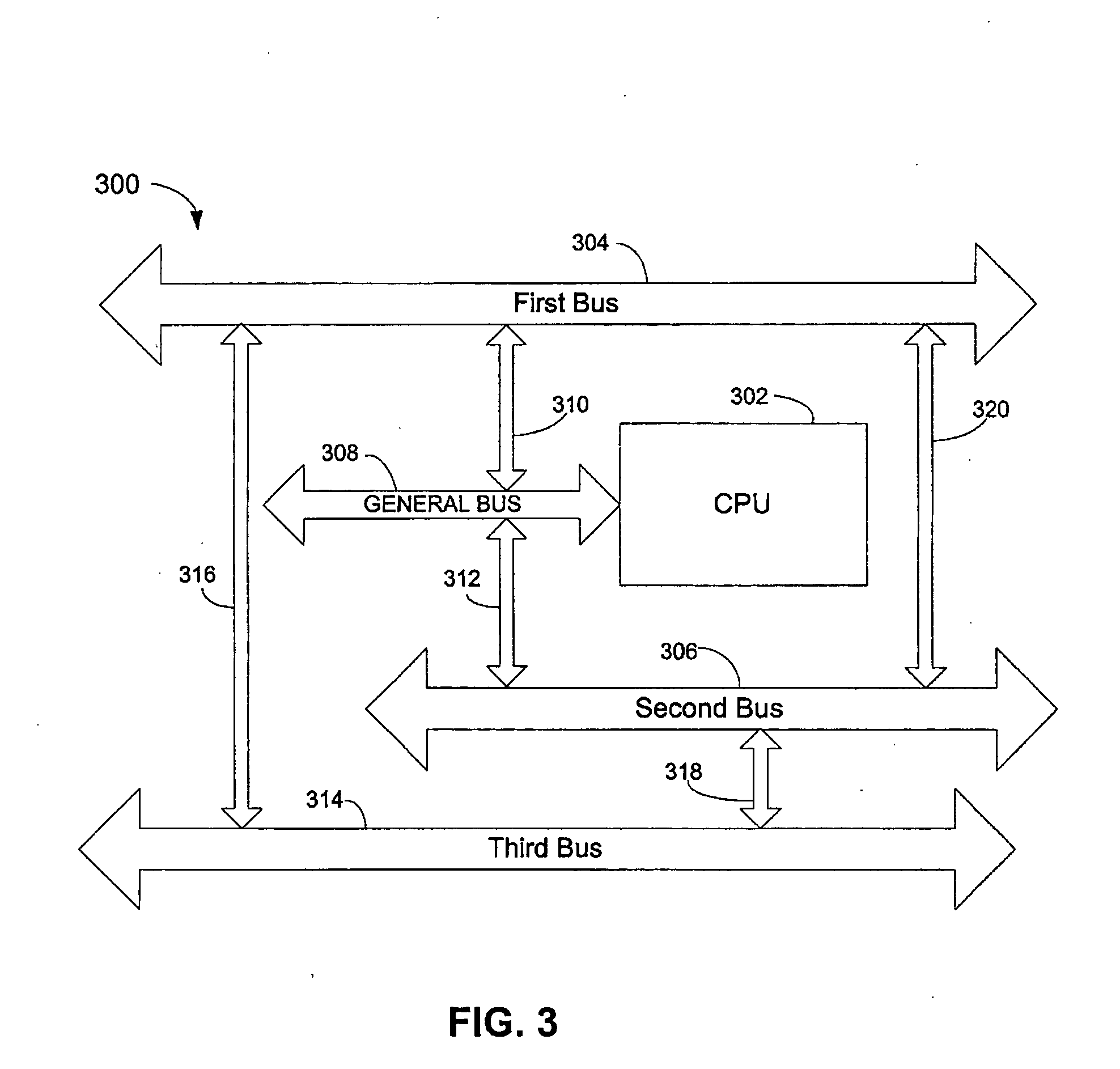
[0022] Throughout this description, the preferred embodiment and examples shown should be considered as exemplars, rather than limitations, of the present invention. The present invention, in accordance with various aspects, is directed to a multi-port processor architecture. The multi-port processor can be employed by system on a chip (SoC) designs to control the system aspects of the SoC.

[0023] Referring to FIG. 1, there is illustrated a system 100 in accordance with an aspect of the present invention. System 100 can be used for SoC designs. The system 100 comprises a CPU 102 that is coupled to a first bus 104 via a bi-directional interface 108. CPU 102 is also connected to a second bus 106 via bi-directional interface 110. A bi-directional interface 112, for example a bus bridge, is used to connect the first bus 104 to the second bus 106.

[0024] Optionally, bus 104 and / or bus 106 can be connected to a memory. For example, if a memory is coupled to the bus 104, then CPU 102 can u...


PUM


Abstract

A multi-port processor architecture having a first bus, a second bus and a central processing unit. The central processing unit having a first and second ports coupled to first and second busses respectively. A first bus to second bus bi-directional interface couples the first bus to the second bus. Optionally, the first bus or the second bus can be connected to a memory. The architecture can include a third bus with a third bus to first bus bi-directional interface connecting the third bus to the first bus and a third bus to second bus bi-directional interface connecting the third bus to the second bus. If there are additional bus systems, the Nth port (where N is an integer greater than 2) is connected to the Nth port. The buses use bi-directional interfaces to communicate with each other without using CPU or memory resources, reducing memory access latency.

Description

BACKGROUND OF THE INVENTION [0001] The present invention relates generally to computer bus architectures and to system-on-a-chip architectures with multi-port processors, including but not limited to embedded processors, application specific integrated circuits (ASICS), Field Programmable Arrays (FPGAs) and other programmable devices. [0002] System-on-a-chip (SoC) design allows a designer to create complex silicon systems from smaller working blocks or systems. By providing a method for easily supporting proprietary functionality in a larger context that in a larger context that includes many existing design pieces, SoC design facilitates the use of silicon design for many systems. There are three views of traffic for a design which are important to differentiate, a memory centric view, a processor centric view and an input / output (I / O) view. Traditionally, prior art systems tend to be processor centric and not balanced. It is desirable that an SoC does not compromise one view over ...

Claims


Application Information

Patent Timeline
Patent Type & Authority Applications(United States)
IPC IPC(8): G06F13/36
CPCG06F13/4027
Inventor FILOR, LUTZ GERHARD EDUARD
Owner TOSHIBA AMERICA ELECTRONICS COMPONENTS
Why Eureka
Try Eureka