Touch display panel and fabrication method thereof, and display device

Active Publication Date: 2016-03-03
BOE TECH GRP CO LTD +1
View PDF3 Cites 1 Cited by
  • Summary
  • Abstract
  • Description
  • Claims
  • Application Information

AI Technical Summary

Benefits of technology

[0009]In the array substrate, the display panel and the display device according to the embodiments of the invention, two pixel electrode layers that are in different layers are provided. Therefore, the area of each pixel electrode can be incr

Problems solved by technology

If the pixel electrodes of adjacent pixels are too close to each other, the pixel electrodes of adjacent pixels may be not completely separated from each other due to the limitation of the precision of the etching process, and thereby connections between pixel electrodes of adjacent pixels are caused.
If the connections bet

Method used


Image

  • Touch display panel and fabrication method thereof, and display device
  • Touch display panel and fabrication method thereof, and display device
  • Touch display panel and fabrication method thereof, and display device

Examples


Example

[0022]In order to make objects, technical details and advantages of the embodiments of the invention apparent, the technical solutions of the embodiment will be described in a clearly and fully understandable way in connection with the drawings related to the embodiments of the invention. It is obvious that the described embodiments are just a part but not all of the embodiments of the invention. Based on the described embodiments herein, those skilled in the art can obtain other embodiment(s), without any inventive work, which should be within the scope of the invention.

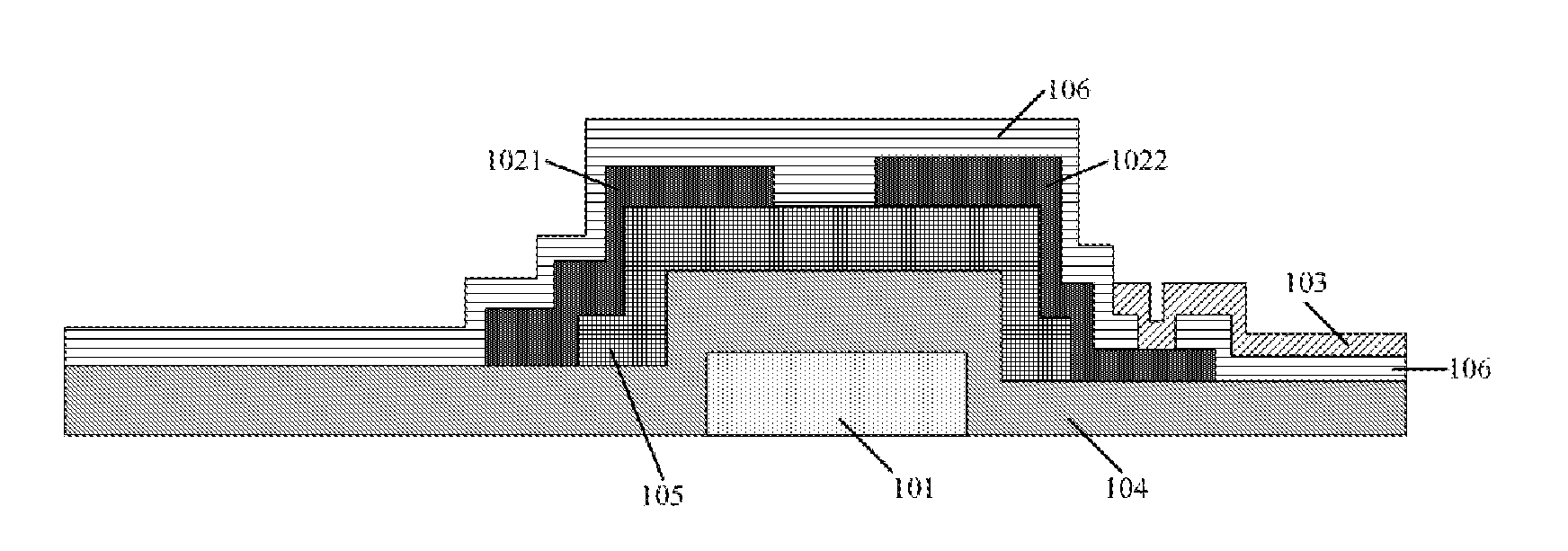
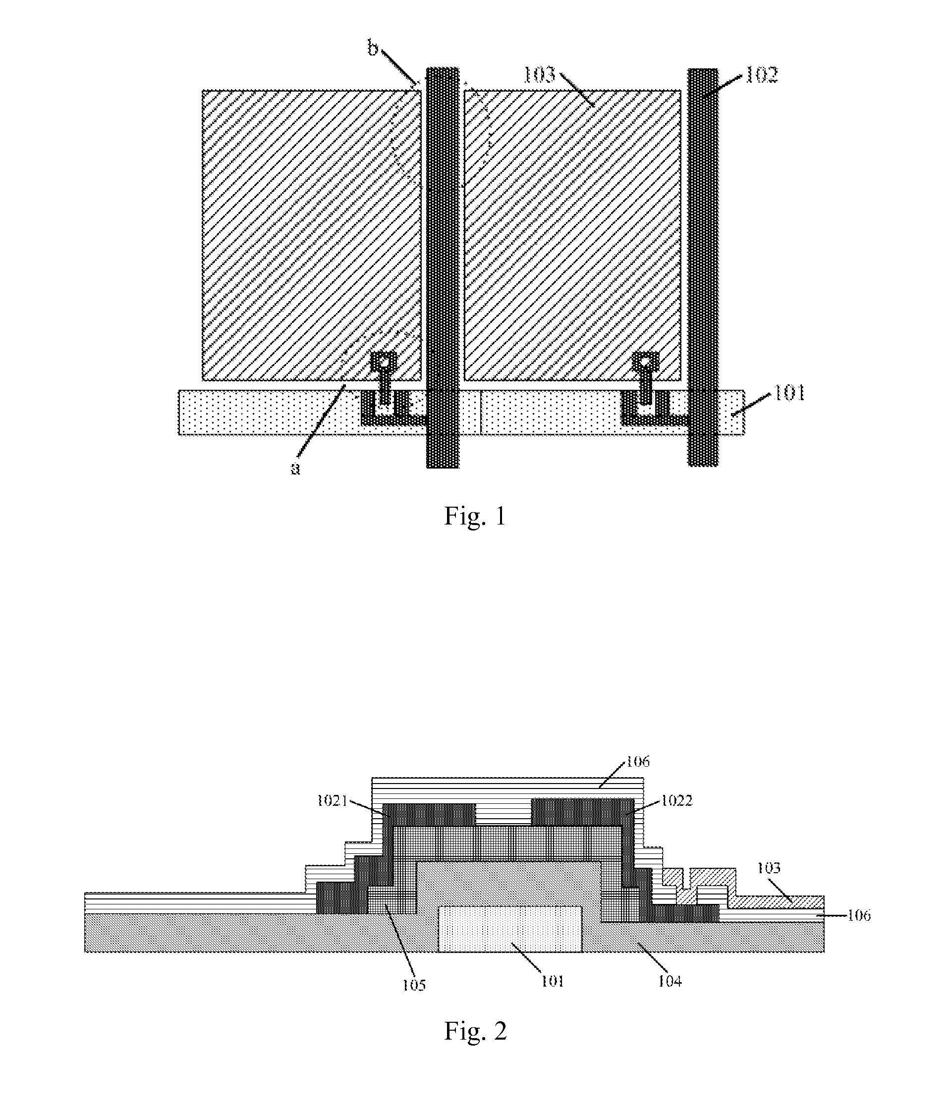
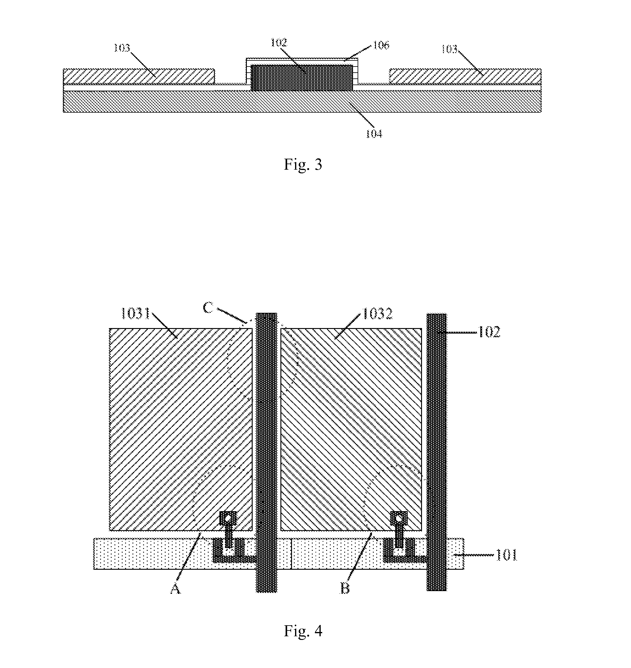
[0023]Embodiments of the invention provide an array substrate comprising a pixel electrode layer. The pixel electrode layer comprises a first pixel electrode layer, a second pixel electrode layer and an insulation layer provided between the first pixel electrode layer and the second pixel electrode layer, the insulation layer insulates the first pixel electrode layer from the second pixel electrode layer, and a pixe...


PUM


Abstract

Embodiments of the invention provide an array substrate, a display panel and a display device. The array substrate comprises a pixel electrode layer. The pixel electrode layer comprises a first pixel electrode layer, a second pixel electrode layer and an insulation layer (104) provided between the first pixel electrode layer and the second pixel electrode layer, the insulation layer (104) insulates the first pixel electrode layer from the second pixel electrode layer, and a pixel electrode (1031) of the first pixel electrode layer and a pixel electrode (1032) of the second pixel electrode layer are alternately arranged.

Description

TECHNICAL FIELD[0001]Embodiments of the invention relate to an array substrate, a display panel and a display device.BACKGROUND[0002]With the wide application of the liquid crystal display device, users raise higher and higher requirements for the liquid crystal display device, especially in terms of increasing the aperture ratio. The “aperture ratio” refers to the ratio of an area of a portion of a pixel where light is transmitted to the entire area of the pixel without considering the wiring portion and the transistor portion (which are generally blocked by a black matrix) of the pixel. The higher the aperture ratio is, the more the light is transmitted.[0003]At present, a pixel electrode layer in the liquid crystal display device is formed by a sputtering process after forming a passivation layer. The whole pixel electrode layer is provided in a same plane, i.e. it belongs to a same layer. FIG. 1 is a schematic view illustrating a pixel structure of a conventional array substrate...

Claims


Application Information

Patent Timeline
IPC IPC(8): G02F1/1343G02F1/1333G02F1/1362G02F1/1368G09G3/36
CPCG02F1/134309G09G3/3648G09G3/3659G02F1/1368G09G2300/0809G02F1/136286G02F1/133345G09G2300/0426G09G2310/02G02F1/136227G02F1/136213H01L27/1214G02F2201/123
Inventor JIANG, WENBOCHEN, XIAOCHUANLI, YUEXUE, HAILIN
Owner BOE TECH GRP CO LTD
Why Eureka
Try Eureka