Active matrix organic light emitting device having series thin film transistor, and fabrication method therefor

Active Publication Date: 2005-03-03
SAMSUNG DISPLAY CO LTD
View PDF9 Cites 1 Cited by
  • Summary
  • Abstract
  • Description
  • Claims
  • Application Information

AI Technical Summary

Benefits of technology

[0010] The present invention provides a series TFT capable of reducing a design rule limitation and increasing an aperture ratio.
[0

Problems solved by technology

Because these two contact holes are required to be formed on the substrate, this increases the size of the area that the pixel driving circuit occupies, which adversely impacts the ability to

Method used


Image

  • Active matrix organic light emitting device having series thin film transistor, and fabrication method therefor
  • Active matrix organic light emitting device having series thin film transistor, and fabrication method therefor
  • Active matrix organic light emitting device having series thin film transistor, and fabrication method therefor

Examples


Example

FIRST EXAMPLE

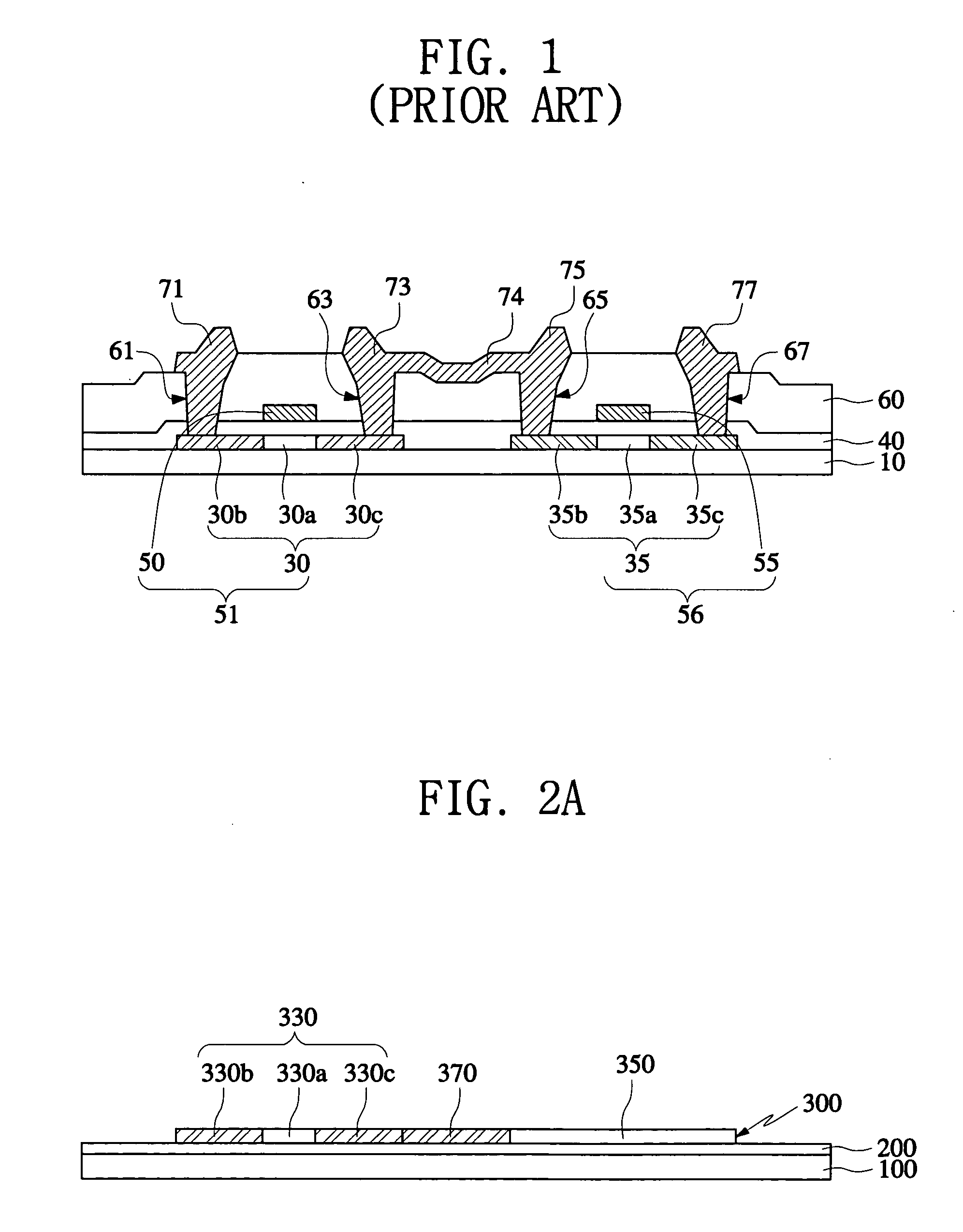
[0057] Referring to FIG. 6A, an amorphous silicon layer, formed on a substrate 800, was subject to crystallization and patterning to form a semiconductor layer 830. A photoresist pattern was then formed on the semiconductor layer 830 to expose a predetermined region of the semiconductor layer 830, and an n-type dopant as a first conductive type impurity was doped using the photoresist pattern as a mask, so that a first region 830d was formed. The photoresist pattern was then removed and a gate insulating layer 840 was formed on the semiconductor layer 830. A gate electrode material was stacked and patterned to form a gate electrode 850 on the gate insulating layer 840. A photoresist pattern was then formed on the substrate where the gate electrode 850 was already formed to expose the region except the first region 830d, and a p-type dopant as a second conductive type impurity was doped using the photoresist pattern and the gate electrode 850 as a mask, so that second r...

Example

SECOND EXAMPLE

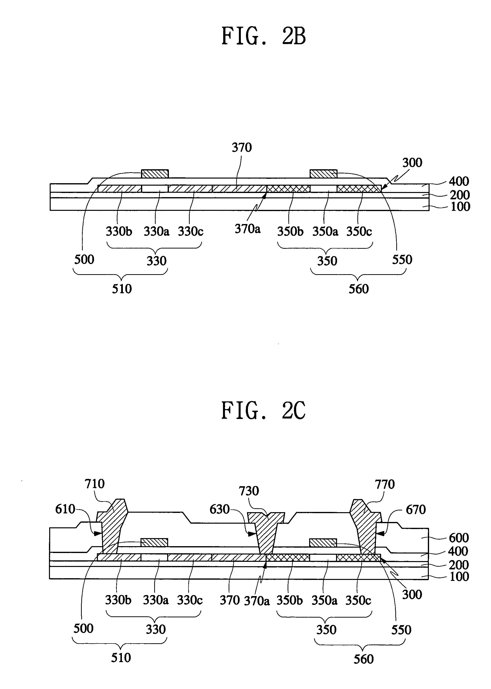
[0060] Referring to FIG. 6B, a semiconductor layer 830 having a first region 830d, second regions 830b and 830c and a channel region 830a, a gate insulating layer 840, a gate electrode 850, and an interlayer 860 were formed on a substrate 800 using the same method as the first example.

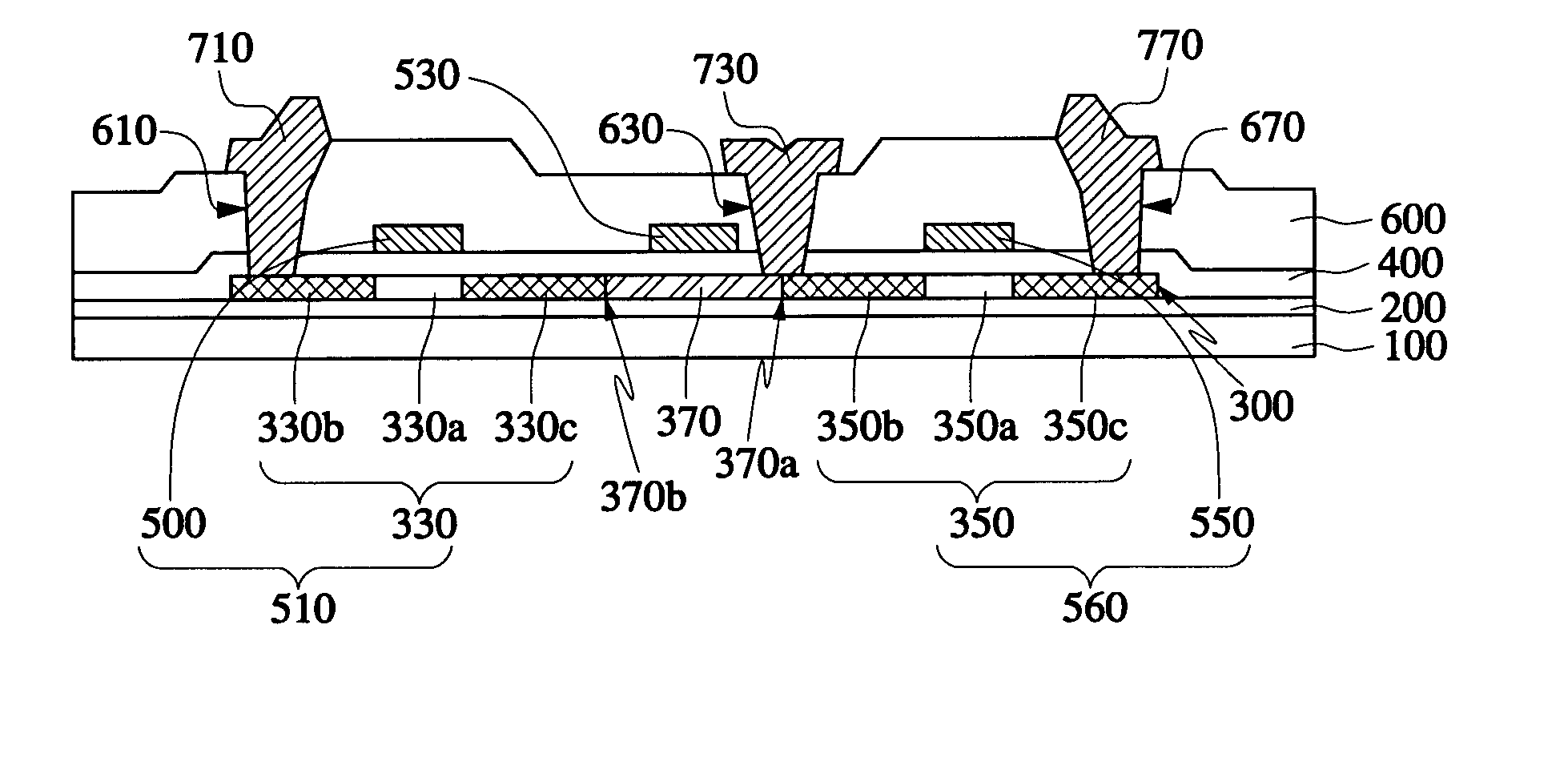
[0061] The first S / D contact hole 863, which exposes a contact surface 830e, and the second S / D contact hole 867, whichexposes the second region 830c, were then formed within the interlayer 860 and the gate insulating layer 840. A conductive layer was then stacked on the substrate where the contact holes were already formed and patterned, thereby forming the first S / D electrode 873, contacted with the contact surface 830e, and the second S / D electrode 877, contacted with the second region 830c, thereby fabricating the TFT. This TFT has the connecting electrode (730 of FIG. 2C) in the series TFT in accordance with the exemplary embodiment of the present invention described with reference...


PUM


Abstract

The series TFT comprises a semiconductor layer including a first body, a second body and a connecting portion serially connecting the first body to the second body. The first body has a first channel region and first source/drain regions positioned at both sides of the first channel region. The second body has a second channel region and second source/drain regions positioned at both sides of the second channel region. And the connecting portion is interposed between the first source/drain region and the second source/drain region to serially connect the first body to the second body and having a conductive type different from that of at least one of the first source/drain region and the second source/drain region. A first gate is positioned to correspond to the first channel region, and a second gate is positioned to correspond to the second channel region. An active matrix OLED can be manufactured using such series TFTs.

Description

CROSS-REFERENCE TO RELATED APPLICATION [0001] This application claims the benefit of Korean Patent Application No. 2003-61587, filed on Sep. 3, 2003, which is hereby incorporated by reference for all purposes as if fully set forth herein. BACKGROUND OF THE INVENTION [0002] 1. Field of the Invention [0003] The present invention relates to a thin film transistor, an organic light emitting device (OLED) comprising the same, and a method for fabricating the OLED and, more particularly, to a series thin film transistor, an active matrix OLED comprising the same, and a method for fabricating the active matrix OLED. [0004] 2. Discussion of the Related Art [0005] Typically, an OLED is an emissive display of a fluorescent organic compound that has been electrically excited to emit light. Depending upon how the display pixels are driven, OLEDs are classified as either passive or active matrix (AM) OLEDs. In an AM OLED, each pixel is driven by its own pixel driving circuit. The AM OLED uses le...

Claims


Application Information

Patent Timeline
IPC IPC(8): H01L21/77H05B33/10H01L21/8234H01L21/8238H01L21/84H01L27/06H01L27/08H01L27/092H01L27/12H01L27/32H01L29/786H01L51/50H05B33/00
CPCH01L27/3262H01L27/1214H01L27/127H10K59/1213H05B33/00
Inventor KWAK, WON-KYU
Owner SAMSUNG DISPLAY CO LTD
Why Eureka
Try Eureka