Method of forming fine patterns of semiconductor device

a technology of semiconductor devices and fine patterns, applied in the field of semiconductor devices, can solve the problems of reducing complicated layout of the mask pattern for this trimming process, and requiring further reduction of the design rule of the nand flash memory device, so as to simplify the trimming process and remove unnecessary portions. , the effect of high density

Active Publication Date: 2009-10-22
SAMSUNG ELECTRONICS CO LTD
View PDF3 Cites 59 Cited by
  • Summary
  • Abstract
  • Description
  • Claims
  • Application Information

AI Technical Summary

Benefits of technology

[0011]The present invention provides a method of forming fine patterns of a semiconductor device, in which, when conductive lines for defining a cell array region of the semiconductor device are integrally formed with contact pads for connecting the conductive lines to a peripheral circuit, fine conductive patterns designed at high density can be formed with various pitches according to a reduced design rule by simplifying a trimming process for removing unnecessary portions.

Problems solved by technology

However, recently, further reduction of the design rule of the NAND flash memory device is required in order to shrink the chip size.
However, in such a conventional NAND flash memory device, a configuration of contact pads for peripheral circuit connections connected to word lines and bit lines is minute and complicated, and thus, a layout of a mask pattern for this trimming process is complicated.
In particular, the design rule of the NAND flash memory device is greatly reduced according to a recent market demand, and pattern sizes of word lines and bit lines that constitute the NAND flash memory device are becoming more minute, and accordingly, the configuration of the contact pads for peripheral circuit connections connected to the word lines and the bit lines become even more minute and complicated.
Thus, the layout of a mask pattern for a trimming process is also minute and complicated.
Thus, due to the possibility of misalignment occurring during performance of an aligning process and due to various parameters used in an etching process, problems such as removal of patterns in necessary regions or generation of undesired shapes of patterns after a trimming process may be generated.

Method used


Image

  • Method of forming fine patterns of semiconductor device
  • Method of forming fine patterns of semiconductor device
  • Method of forming fine patterns of semiconductor device

Examples


first embodiment

[0048]FIGS. 4A through 4K are cross-sectional views for explaining a method of forming fine patterns of the semiconductor device of FIG. 3, according to the present invention.

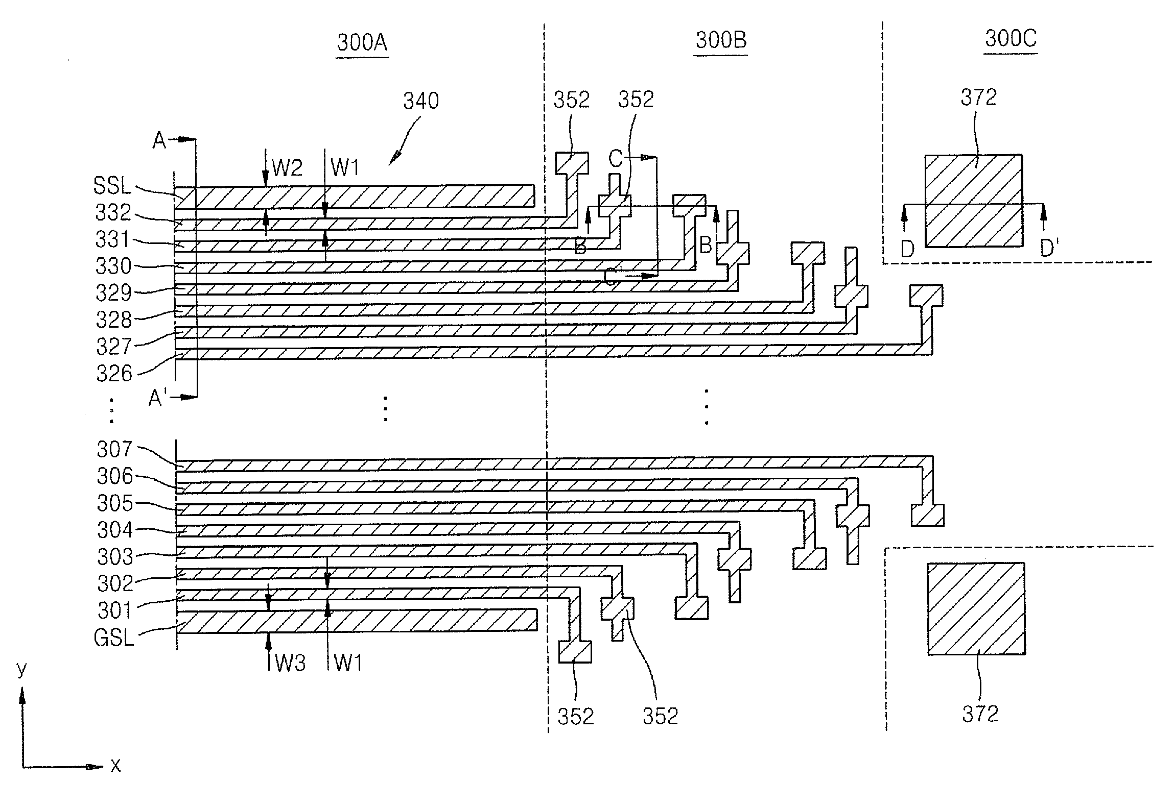
[0049]FIGS. 5A through 5F are plan views of layouts of a major part of the semiconductor device of FIG. 3, which is explained in processes of FIGS. 4A through 4K. FIGS. 5A through 5F illustrate only the single memory cell block 340 of FIG. 3.

[0050]FIGS. 4A through 4K illustrate cross-sections taken along lines A-A′, B-B′, C-C′, and D-D′ of FIG. 3, according to a process sequence. In FIGS. 4A through 4K and FIGS. 5A through 5F, the same reference characters as those of FIG. 3 denote like elements, and thus their description will be omitted. In FIGS. 4A through 4K, the memory cell region 300A is represented as “CELL”, the contact region 300B is represented as “CONTACT”, and the peripheral circuit region 300C is represented as “PERI”.

[0051]Referring to FIGS. 4A and 5A, first, a substrate 500, for example, a silico...

second embodiment

[0084]FIGS. 6A through 6F are cross-sectional views for explaining a method of forming fine patterns of the semiconductor device of FIG. 3, according to the present invention.

[0085]In FIGS. 6A through 6F, the same reference characters as those of FIGS. 3, 4A through 4K, and 5A through 5F denote like elements, and thus their description will be omitted.

[0086]Referring to FIG. 6A, in a method as described above with reference to FIGS. 4A, 5A, and 4B, the conductive layer 530, the first hard mask layer 532, and the second hard mask layer 534 are sequentially formed on the substrate 500, and the mold mask patterns 540 and the mask layer 550 are then formed on the second hard mask layer 534.

[0087]Thereafter, the gap-fill protection film 560 is formed on the mask layer 550.

[0088]The gap-fill protection film 560 may be formed according to a process similar to that described above with reference to FIG. 4D. In other words, the gap-fill protection film 560 may be formed to completely cover t...

third embodiment

[0103]FIGS. 7A and 7B are cross-sectional views for explaining a method of forming fine patterns of the semiconductor device of FIG. 3, according to the present invention.

[0104]In FIGS. 7A and 7B, the same reference characters as those of FIGS. 3, 4A through 4K, 5A through 5F, and 6A through 6F denote like elements, and thus their description will be omitted.

[0105]Referring to FIG. 7A, in a method similar to that described above with reference to FIGS. 6A through 6D, the conductive layer 530, the first hard mask layer 532, and the second hard mask layer 534 are sequentially formed on the substrate 500, and a plurality of butted mask pattern pairs 550b are then formed on the second hard mask layer 534.

[0106]Thereafter, the butted mask pattern pairs 550b are entirely etched back until the horizontal extensions 550h of the butted mask pattern pairs 550b are completely removed. Thus, portions of the upper surface of the second hard mask layer 534, which are located below the horizontal ...


PUM

PropertyMeasurementUnit
temperatureaaaaaaaaaa

Abstract

A method of forming fine patterns of a semiconductor device, in which a plurality of conductive lines formed in a cell array region are integrally formed with contact pads for connecting the conductive lines to a peripheral circuit. In this method, a plurality of mold mask patterns, each including a first portion extending in a first direction and a second portion which is integrally formed with the first portion and extends in a second direction, are formed within a cell block on a substrate comprising a film which is to be etched. A first mask layer covering sidewalls and an upper surface of each of the plurality of mold mask patterns is formed on the substrate. First mask patterns are formed by partially removing the first mask layer so that a first area of the first mask layer remains and a second area of the first mask layer is removed. The first area of the first mask layer covers sidewalls of adjacent mold mask patterns from among the plurality of mold mask patterns by being located between the adjacent mold mask patterns, and the second area of the first mask layer covers portions of the sidewalls of the plurality of mold mask patterns, the portions corresponding to an outermost sidewall of a mold mask pattern block.

Description

CROSS-REFERENCE TO RELATED PATENT APPLICATION[0001]This application claims the benefit of Korean Patent Application No. 10-2008-0035819, filed on Apr. 17, 2008, in the Korean Intellectual Property Office, the disclosure of which is incorporated herein in its entirety by reference.BACKGROUND OF THE INVENTION[0002]The present invention relates generally to semiconductor devices and, more particularly, to semiconductor device manufacturing.[0003]In a cell array region of a semiconductor device, a plurality of conductive lines for defining unit cells, for example, a plurality of word lines and a plurality of bit lines, are arranged in a predetermined direction.[0004]FIG. 1 is a block diagram of a memory cell array 100 of a conventional NAND flash memory device, which is a type of non-volatile memory device, and an X-decoder 110 and a Y-decoder 120, which are peripheral circuits of the memory cell array 100. FIG. 2 is a circuit diagram of a structure of the memory cell array 100.[0005]Re...

Claims


Application Information

Patent Timeline
Patent Type & Authority Applications(United States)
IPC IPC(8): H01L21/302G03F7/20
CPCH01L21/0337H01L21/32139H01L27/11575H01L27/11548H01L27/11573H01L27/11526H10B41/50H10B41/40H10B43/50H10B43/40
Inventor SIM, JAE-HWANGPARK, SANG-YONGLEE, YOUNG-HO
Owner SAMSUNG ELECTRONICS CO LTD
Why Eureka
Try Eureka