Capacitor insulating film, method for fabricating the same, capacitor element, method for fabricating the same, semiconductor memory device, and method for fabricating the same

a capacitor insulating film and capacitor element technology, applied in the direction of fixed capacitor details, fixed capacitors, coatings, etc., can solve the problems of reducing the ferroelectric property, unable to obtain sufficient excellent ferroelectric properties, and the capacitor insulating film composed of the ferroelectric film formed by the forgoing conventional method does not exhibit excellent properties, etc., to achieve excellent polarization properties, reduce design rules, and excellent electric properties

Inactive Publication Date: 2009-12-31
PANASONIC CORP
View PDF13 Cites 3 Cited by
  • Summary
  • Abstract
  • Description
  • Claims
  • Application Information

AI Technical Summary

Benefits of technology

[0014]In view of the foregoing, an object of the present invention is to provide a capacitor insulating film having a sufficiently excellent polarization property even when it is miniaturized. Another object of the present invention is to provide a capacitor element which allows a reduction in design rules and also has excellent electric properties and provide a semiconductor memory device having the capacitor element.

Problems solved by technology

However, a capacitor element having the capacitor insulating film composed of the ferroelectric film formed by the foregoing conventional method does not exhibit excellent properties.
However, since the SrBi2Ta2O9 film does not hold a polarization component in the C-axis direction, a sufficiently excellent ferroelectric property cannot be obtained.
This further degrades the ferroelectric property.
Thus, it has been difficult in accordance with the conventional method to provide a capacitor element which has been miniaturized and also has a sufficiently excellent polarization property.
In other words, it has been difficult to provide a capacitor element which both allows a reduction in design rules and has excellent electric properties.

Method used


Image

  • Capacitor insulating film, method for fabricating the same, capacitor element, method for fabricating the same, semiconductor memory device, and method for fabricating the same
  • Capacitor insulating film, method for fabricating the same, capacitor element, method for fabricating the same, semiconductor memory device, and method for fabricating the same
  • Capacitor insulating film, method for fabricating the same, capacitor element, method for fabricating the same, semiconductor memory device, and method for fabricating the same

Examples


embodiment 1

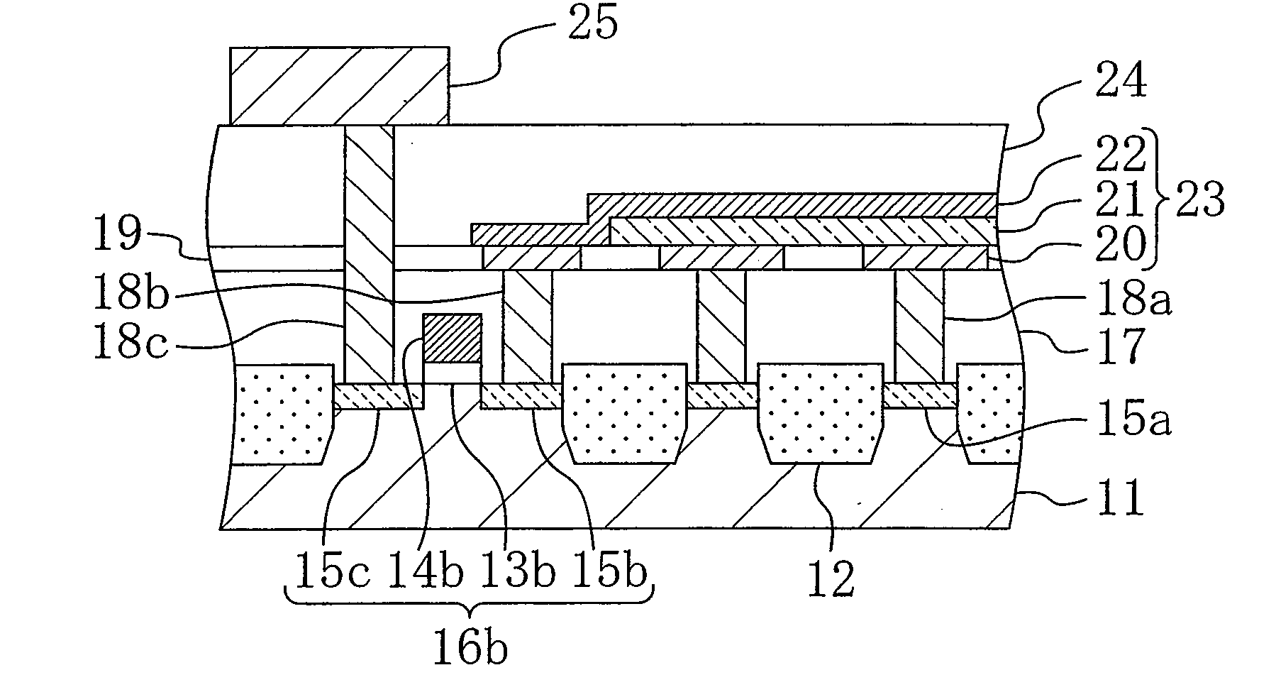
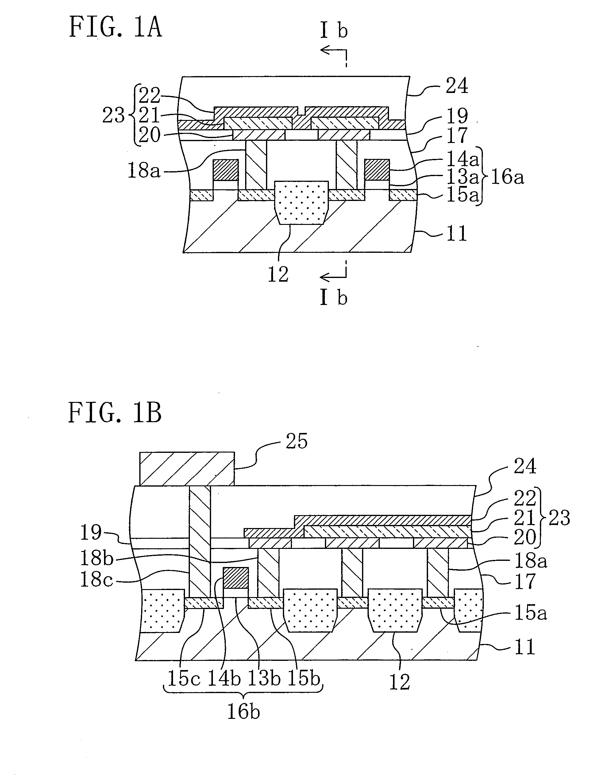
[0075]A description will be given herein below to a capacitor insulating film, a fabrication method therefor, a capacitor element using the capacitor insulating film, a fabrication method therefor, a semiconductor memory device using the capacitor insulating film, and a fabrication method therefor, each according to a first embodiment of the present invention with reference to the drawings.

[0076]The description will be given first to the respective structures of the capacitor insulating films, the capacitor elements comprising the capacitor insulating films, and the semiconductor memory devices comprising the capacitor insulating films, each according to the first embodiment with reference to the drawings.

[0077]FIGS. 1A and 1B are cross-sectional views showing the structures of the capacitor insulating films, the capacitor elements using the capacitor insulating films, and the semiconductor memory devices using the capacitor insulating films, each according to the first embodiment, ...

embodiment 2

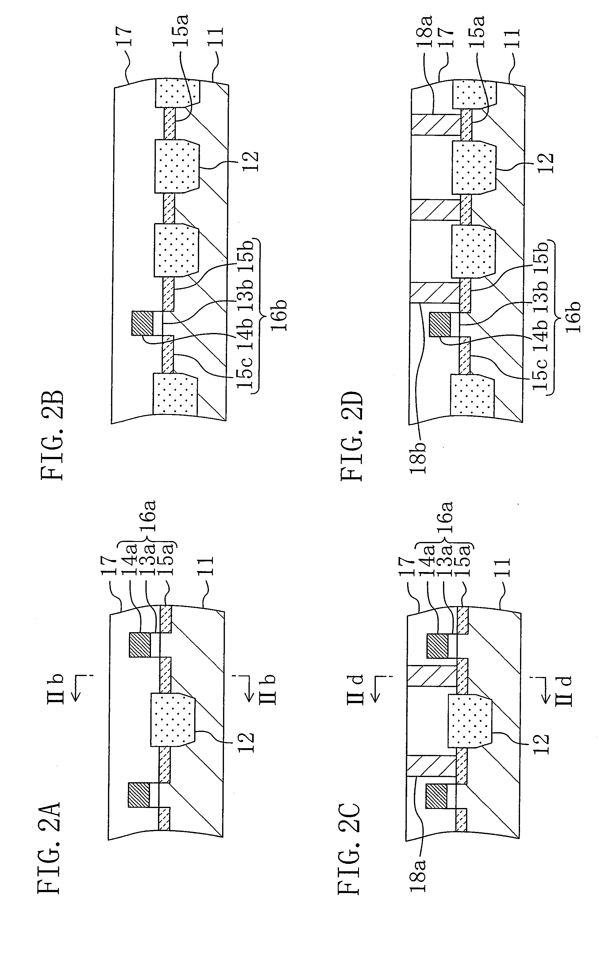
[0122]A description will be given herein below to a capacitor insulating film, a fabrication method therefor, a capacitor element using the capacitor insulating film, a fabrication method therefor, a semiconductor memory device using the capacitor insulating film, and a fabrication method therefor each according to a second embodiment of the present invention with reference to the drawings. The second embodiment will describe the case where capacitor elements each having a concave-type three-dimensional structure are formed as shown in FIG. 8, which will be described later.

[0123]The description will be given first to the respective structures of the capacitor insulating films, the capacitor elements using the capacitor insulating films, and the semiconductor memory device using the capacitor insulating films. each according to the second embodiment with reference to the drawings.

[0124]FIG. 8 is a principal-portion of cross-sectional view showing the structures of the capacitor insul...


PUM

PropertyMeasurementUnit
temperatureaaaaaaaaaa
grain sizeaaaaaaaaaa

Abstract

A capacitor insulating film is composed of a ferroelectric film formed on a substrate and containing an element functioning as a crystal nucleus which allows the growth of a crystal in a random crystal orientation.

Description

CROSS-REFERENCE TO RELATED APPLICATIONS[0001]The teachings of Japanese Patent Application JP 2004-339472, filed Nov. 24, 2004, are entirely incorporated herein by reference, inclusive of the specification, drawings, and claims.BACKGROUND OF THE INVENTION[0002]The present invention relates to a capacitor insulating film made of a ferroelectric material, a method for fabricating the same, a capacitor element using a capacitor insulating film made of a ferroelectric material, a method for fabricating the same, a semiconductor memory device having a capacitor element using a capacitor insulating film made of a ferroelectric material, and a method for fabricating the same.[0003]In recent years, vigorous research and development have been conducted on a ferroelectric film having a characteristic of spontaneous polarization with a view of commercializing a nonvolatile RAM capable of high-speed read / write operations at an unprecedentedly low voltage. To implement a megabit-class semiconduct...

Claims


Application Information

Patent Timeline
Patent Type & Authority Applications(United States)
IPC IPC(8): H01L27/06H01G4/06B05D5/12H01L21/8239
CPCC23C16/40C23C16/56H01L21/31691H01L28/65H01L27/11507H01L28/55H01L27/11502H01L21/02205H01L21/02271H01L21/02197H10B53/30H10B53/00H10B12/00H01L21/02356
Inventor HAYASHI, SHINICHIRONASU, TORU
Owner PANASONIC CORP
Why Eureka
Try Eureka