

Display device and manufacturing method thereof
a technology of a display device and a manufacturing method, which is applied in the direction of semiconductor devices, instruments, electrical devices, etc., can solve the problems of reducing image quality and pixel luminance, and achieve the effects of reducing or eliminating the generation of parasitic capacitance, preventing the voltage of the driving gate electrode from being undesired, and ensuring the capacitance of the capacitor
- Summary
- Abstract
- Description
- Claims
- Application Information
AI Technical Summary
Benefits of technology
Problems solved by technology
Method used
Image

Examples
Embodiment Construction
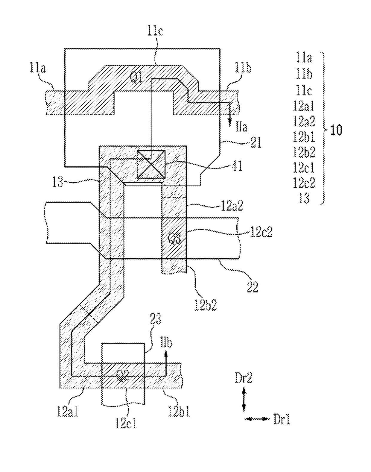
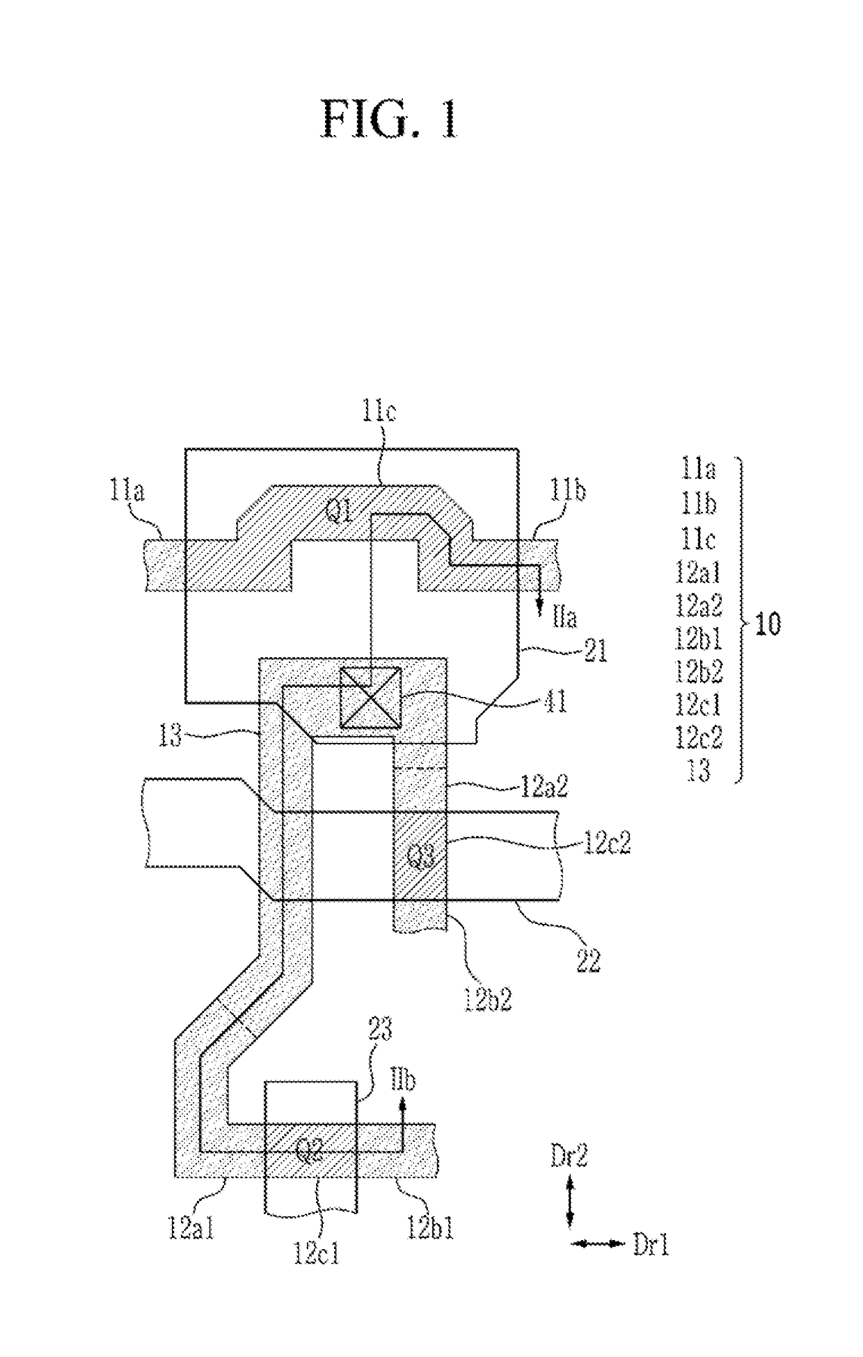
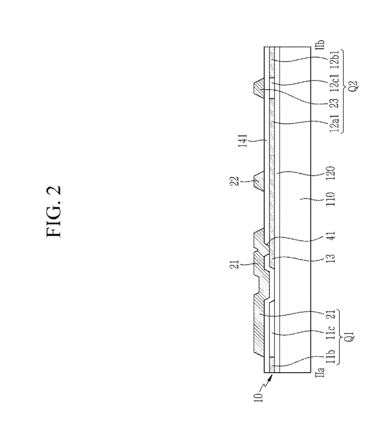
[0057]Exemplary embodiments of the present invention will be described in more detail below with reference to the accompanying drawings, in which exemplary embodiments of the present invention are shown. As those skilled in the art would realize, the described embodiments may be modified in various different ways, all without departing from the spirit or scope of the present invention.
[0058]In the drawings, the thicknesses of layers, films, panels, or regions may be exaggerated for clarity. Like reference numerals may refer to like elements throughout the specification and drawings. It will be understood that when an element such as a layer, film, region, or substrate is referred to as being “on” another element, it may be directly on the other element or intervening elements may be present. The phrase “in a plan view” means when an object portion is viewed from above, and the phrase “in a cross-section” means when a cross-section taken by vertically cutting an object portion is vie...
PUM
 Abstract
Description
Claims
Application Information