Method for manufacturing material layer, method for manufacturing ferroelectric capacitor using the same, ferroelectric capacitor manufactured by the same method, semiconductor memory device having ferroelectric capacitor and manufacturing method thereof

a manufacturing method and material layer technology, applied in the direction of capacitors, semiconductor devices, electrical equipment, etc., can solve the problems of affecting the operation reliability of the resulting semiconductor memory device, etc., to achieve the effect of improving the operation reliability and sufficient capacitan

Inactive Publication Date: 2008-09-04
KOO JUNE MO +5
View PDF6 Cites 0 Cited by
  • Summary
  • Abstract
  • Description
  • Claims
  • Application Information

AI Technical Summary

Benefits of technology

[0013]Example embodiments provide a method for manufacturing a material layer capable of increasing the deposition rate of a noble metal layer on a ferroelectric layer.
[0014]Example embodiments also provide a method for manufacturing a ferroelectric capacitor having a three-dimensional structure, capable of achieving improved step coverage of an upper electrode and / or achieving larger capacitance using any of the above methods of manufacturing a material layer.
[0016]Example embodiments also provide a semiconductor device and a method thereof, capable of achieving higher integration and / or higher reliability by providing any of the above ferroelectric capacitors.
[0029]According to example embodiments, it is possible to form an upper electrode of noble metal on the entire exposed region of the ferroelectric layer regardless of the shape of the ferroelectric layer. Therefore, the wide contact area between the ferroelectric layer and the upper electrode may be secured, so that the capacitance of the ferroelectric capacitor may be sufficiently secured. Also, methods for manufacturing semiconductor memory devices according to example embodiments may be used to form any of the above-described ferroelectric capacitors. Therefore, because a ferroelectric capacitor having sufficient capacitance may be manufactured when methods for manufacturing the semiconductor memory device are used, the operational reliability of the resulting semiconductor memory devices may be improved.

Problems solved by technology

However, DRAMs may have disadvantages, including volatility and / or requiring periodic refreshes during operation thereof.
However, forming of the capacitor in a three-dimensional structure means that the structure of the capacitor may be more complicated.
Therefore, it may be more difficult to form a capacitor having a three-dimensional structure in higher integration DRAM and FRAM using a conventional deposition method, such as CVD.
However, problems with ALD may occur during a process of forming an electrode on ferroelectric layers formed in a three-dimensional structure.
For example, when forming an upper electrode with predetermined or desired noble metal (e.g., Ir) using ALD on a ferroelectric layer (e.g., lead zirconate titanate (PZT) layer) formed in a trench structure, the ALD may form an Ir layer on a flat region of the ferroelectric layer located between trenches but may not be able to form an Ir layer on inner sides of the trenches.
That is, conventional ALD techniques may not uniformly form an upper electrode having sufficient step coverage on an entire region of the ferroelectric layer having a three-dimensional structure.

Method used


Image

  • Method for manufacturing material layer, method for manufacturing ferroelectric capacitor using the same, ferroelectric capacitor manufactured by the same method, semiconductor memory device having ferroelectric capacitor and manufacturing method thereof
  • Method for manufacturing material layer, method for manufacturing ferroelectric capacitor using the same, ferroelectric capacitor manufactured by the same method, semiconductor memory device having ferroelectric capacitor and manufacturing method thereof
  • Method for manufacturing material layer, method for manufacturing ferroelectric capacitor using the same, ferroelectric capacitor manufactured by the same method, semiconductor memory device having ferroelectric capacitor and manufacturing method thereof

Examples


Embodiment Construction

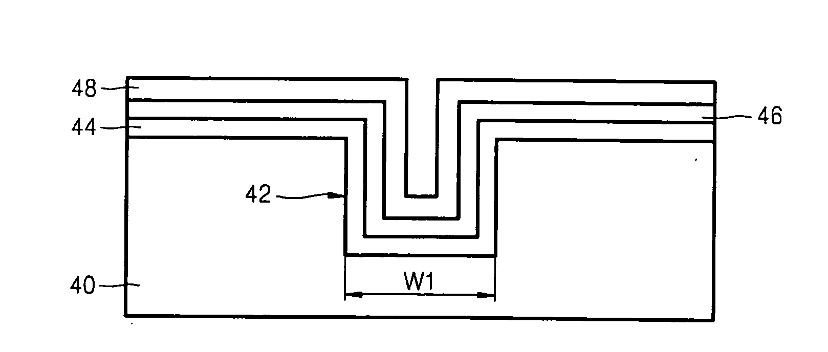
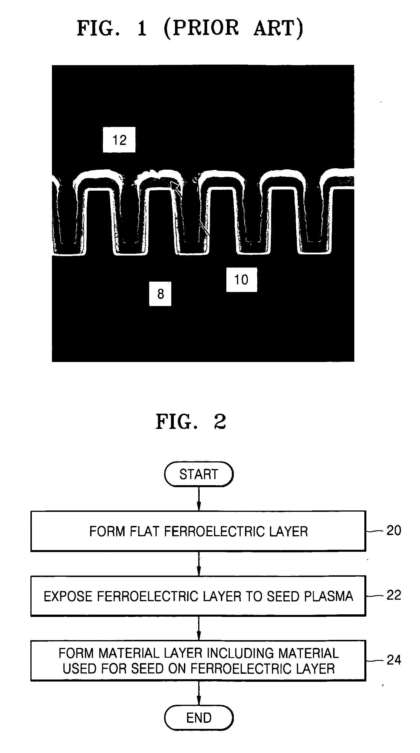
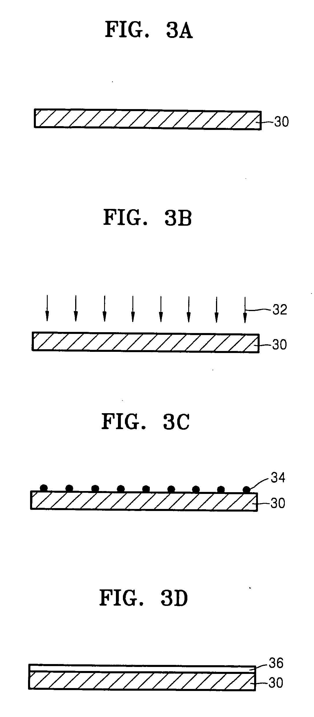
[0042]Example embodiments will now be described more fully with reference to the accompanying drawings. In the drawings, the thicknesses of layers and regions are exaggerated for clarity. Example embodiments will now be described more fully hereinafter with reference to the accompanying drawings. This invention may, however, be embodied in many different forms and should not be construed as being limited to the example embodiments set forth herein. Rather, these example embodiments are provided so that this disclosure will be thorough and complete, and convey the scope of example embodiments to those skilled in the art. Like numbers refer to like elements throughout the specification.

[0043]It will be understood that when an element or layer is referred to as being “on”, “connected to” or “coupled to” another element or layer, it can be directly on, connected or coupled to the other element or layer or intervening elements or layers may be present. In contrast, when an element is ref...


PUM


Abstract

Provided is a method for manufacturing a material layer capable of increasing the deposition rate of a noble metal layer on a ferroelectric layer, a method for manufacturing a ferroelectric capacitor using the same, a ferroelectric capacitor manufactured by the same method, and a semiconductor memory device having the ferroelectric capacitor and a manufacturing method thereof. According to a method for manufacturing the material layer, a ferroelectric layer is formed. The ferroelectric layer may be exposed to seed plasma, and a material layer including a source material of the seed plasma may be formed on a region of the ferroelectric layer exposed to the seed plasma.

Description

PRIORITY STATEMENT[0001]This application claims the benefit of Korean Patent Application No. 10-2005-0063302, filed on Jul. 13, 2005, in the Korean Intellectual Property Office, the disclosure of which is incorporated herein in its entirety by reference.BACKGROUND[0002]1. Field[0003]Example embodiments relate to a method for depositing a material layer, for example, a method for manufacturing a material layer capable of increasing the deposition rate of a noble metal layer on a ferroelectric layer, a method for manufacturing a ferroelectric capacitor using the same, a ferroelectric capacitor manufactured by the same method, and a semiconductor memory device having the ferroelectric capacitor and a manufacturing method thereof.[0004]2. Description of the Related Art[0005]Semiconductor devices may be roughly classified into random access memories (RAMs) having volatility and which are freely read and written, and read only memories (ROMs) having non-volatility and which are read only....

Claims


Application Information

Patent Timeline
Patent Type & Authority Applications(United States)
IPC IPC(8): H01L29/92H01L21/8246
CPCH01L21/31691H01L28/65H01L27/11507H01L27/11502H01L21/02197H01L21/0228H10B53/30H10B53/00H01L27/105H01L21/20H10B12/00
Inventor KOO, JUNE-MOSEO, BUM-SEOKPARK, YOUNG-SOOLEE, JUNG-HYUNSHIN, SANG-MINKIM, SUK-PIL
Owner KOO JUNE MO
Why Eureka
Try Eureka