Thin film deposition via a spatially-coordinated and time-synchronized process

a spatially coordinated, time-synchronized, thin film technology, applied in the direction of plasma technology, sustainable manufacturing/processing, final product manufacturing, etc., can solve the problems of low absorption efficiency of crystalline silicon, inherently slow method, high cost, etc., and achieve high deposition rate and improve photovoltaic efficiency

Inactive Publication Date: 2010-06-17
OVSHINSKY TECH
View PDF13 Cites 119 Cited by
  • Summary
  • Abstract
  • Description
  • Claims
  • Application Information

AI Technical Summary

Benefits of technology

[0023]The instant invention provides a method and apparatus for the plasma deposition of thin film materials. In one embodiment, the invention is directed at the plasma deposition of photovoltaic materials at high deposition rates with improved photovoltaic efficiency by providing a method and apparatus for controlling plasma composition and the timing of the delivery of species to the plasma. The invention recognizes that the plasmas used in prior art deposition processes include species that are detrimental to photovoltaic efficiency.

Problems solved by technology

Crystalline silicon, however, has a number of disadvantages as a solar energy material.
Although high purity crystalline silicon can be achieved and the Czochralski method is amenable to n- and p-type doping, the method is inherently slow, expensive, and energy intensive.
Second, as an indirect gap material, crystalline silicon has a low absorption efficiency.
The thick layers add to the cost of crystalline silicon solar panels, lead to a significant increase in weight, necessitate bulky installation mounts, and make crystalline silicon solar panels rigid and unsuitable for applications requiring a flexible photovoltaic material.
CdTe and CdS suffer from the problem that Cd is a toxic element that requires special disposal procedures.
Although CIGS shows promising solar efficiency, it is difficult to achieve uniform stoichiometry over the large scale substrates required for high-volume manufacturing.
One problem with current plasma-deposited photovoltaic materials is the presence of a high concentration of intrinsic defects in the as-deposited state.
The intrinsic defects include structural defects (e.g. dangling bonds, strained bonds, unpassivated surface states, non-tetrahedral bonding distortions, coordinatively unsaturated silicon or germanium) that create electronic states within the bandgap of the photovoltaic material.
The intrinsic defects are also believed to contribute to a degradation of solar cell performance of amorphous silicon-based photovoltaic materials through the Staebler-Wronski effect.
Excess photo-excited carrier is trapping, recombination, or other dissipation leads to low carrier mobility and reduces the likelihood that carriers are extracted from the material to contribute to an external current.
A drawback of amorphous silicon as a solar energy material is its low hole mobility.
The low hole mobility reduces solar efficiency and makes simple p-n junction devices based on amorphous silicon impractical.
Although the ordered cluster material has desirable properties, current techniques for forming it suffer from low deposition rates.
The low deposition rates needed to achieve high efficiency photovoltaic materials through conventional plasma deposition techniques limit the economic competiveness of photovoltaic materials relative to fossil fuels and motivate a search for new deposition processes.

Method used


Image

  • Thin film deposition via a spatially-coordinated and time-synchronized process
  • Thin film deposition via a spatially-coordinated and time-synchronized process
  • Thin film deposition via a spatially-coordinated and time-synchronized process

Examples


Embodiment Construction

[0034]Although this invention will be described in terms of certain preferred embodiments, other embodiments that are apparent to those of ordinary skill in the art, including embodiments that do not provide all of the benefits and features set forth herein and including embodiments that provide positive benefits for high-volume manufacturing, are also within the scope of this invention. Accordingly, the scope of the invention is defined only by reference to the appended claims.

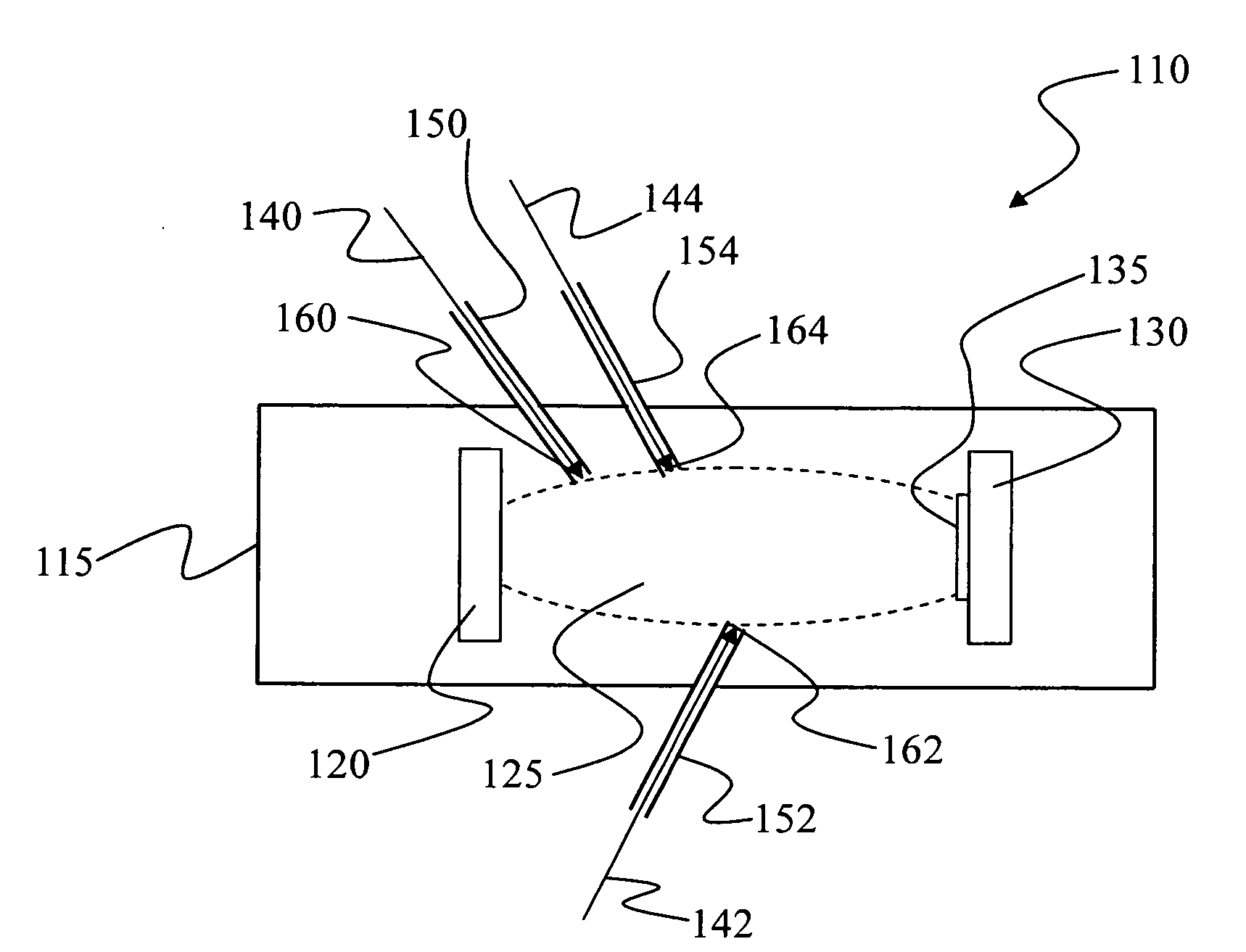
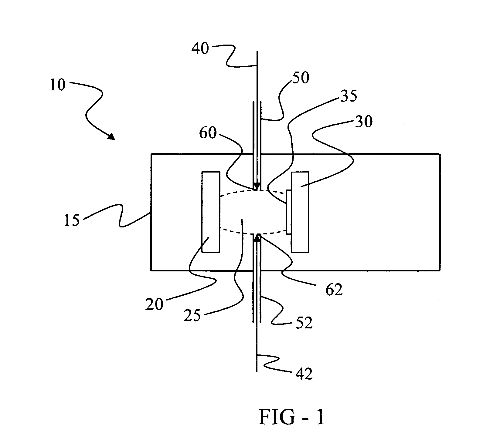
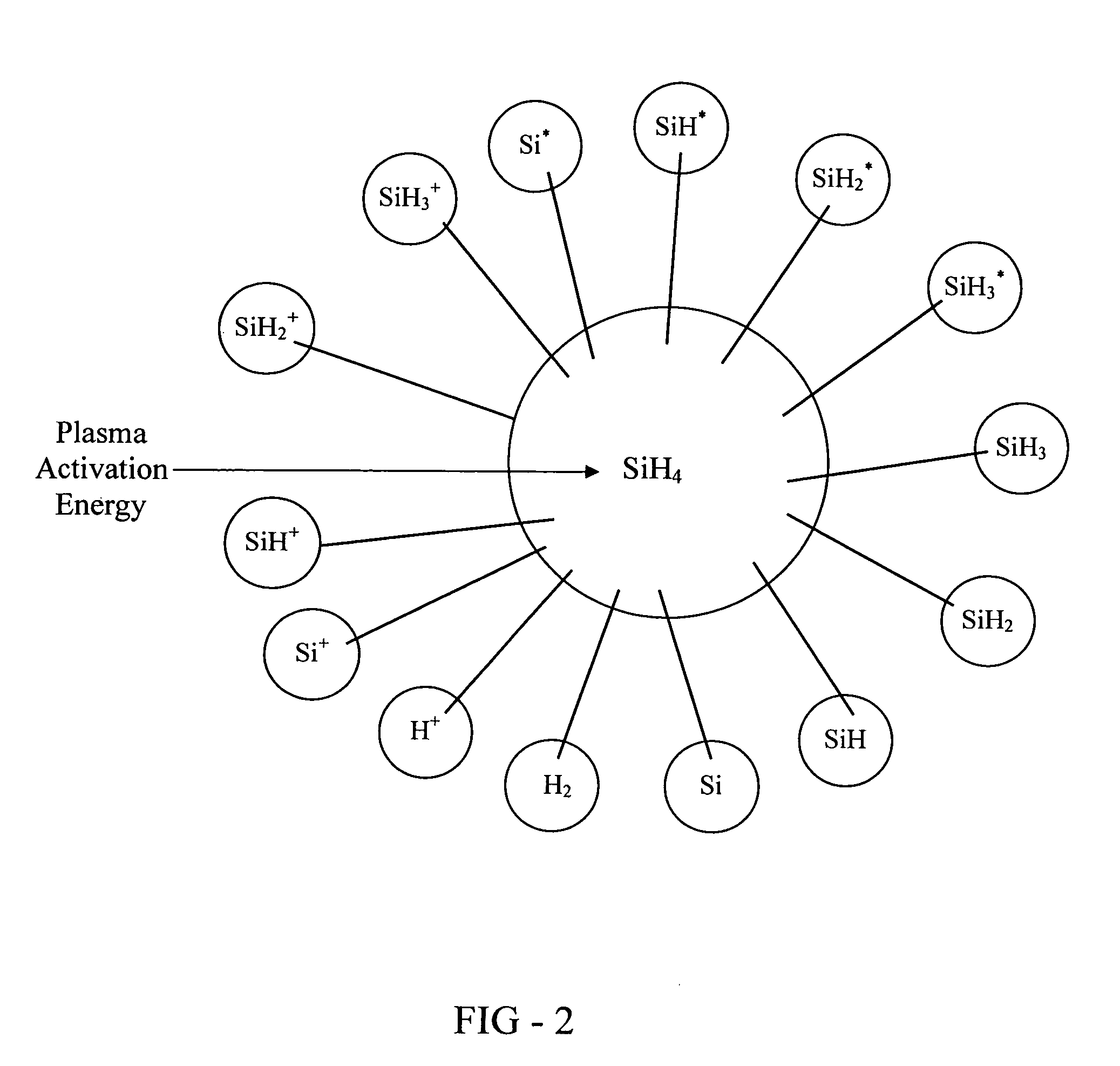
[0035]The instant invention focuses on a plasma deposition process in which the state of the plasma is engineered to optimize the structural and electronic quality of an as-deposited thin film material. In one embodiment, the thin film material is a photovoltaic material. The invention is designed to remedy deficiencies in the plasma that forms naturally in a conventional plasma deposition process. In the prior art, a plasma is normally formed by first delivering a molecular precursor and a carrier gas to a c...


PUM

PropertyMeasurementUnit
electric fieldaaaaaaaaaa
cross-sectional dimensionaaaaaaaaaa
dimensionaaaaaaaaaa

Abstract

A deposition system and process for the formation of thin film materials. In one embodiment, the process includes forming an initial plasma from a first material stream and allowing the plasma to evolve in space and/or time to extinguish species that are detrimental to the quality of the thin film material. After the initial plasma evolves to an optimum state, a second material stream is injected into the deposition chamber to form a composite plasma that contains a distribution of species more conducive to formation of a high quality thin film material. The deposition system includes a deposition chamber having a plurality of delivery points for injecting two or more streams (source materials or carrier gases) into a plasma region. The delivery points are staggered in space to permit an upstream plasma formed from a first material stream deposition source material to evolve before combining a downstream material stream with the plasma. Injection of different material streams is also synchronized in time. The net effect of spatial coordination and time synchronization of material streams is a plasma whose distribution of species is optimized for the deposition of a thin film photovoltaic material at high deposition rates. Delivery devices include nozzles and remote plasma sources.

Description

FIELD OF INVENTION[0001]This invention relates to the plasma deposition of thin film materials. More particularly, this invention relates to deposition of thin films from a plasma composed of a distribution of compatible species carefully selected to form a photovoltaic material with high conversion efficiency. Most particularly, this invention relates to a plasma deposition process based on a deposition apparatus that includes multiple points of delivery, where the points of delivery provide each of one or more deposition species at preferential positions along the apparatus and where the delivery of species is coordinated in space and synchronized in time to promote stabilization of the optimum combination of species for deposition.BACKGROUND OF THE INVENTION[0002]Concern over the depletion and environmental impact of fossil fuels has stimulated strong interest in the development of alternative energy sources. Significant investments in areas such as batteries, fuel cells, hydroge...

Claims


Application Information

Patent Timeline
Patent Type & Authority Applications(United States)
IPC IPC(8): C23C16/513H05H1/24H05H1/34H05H1/42
CPCC23C16/24C23C16/452C23C16/455Y02E10/50H01L31/202H05H1/42C23C16/50Y02P70/50H01L21/205H01L31/18H01L31/04
Inventor OVSHINSKY, STANFORD R.
Owner OVSHINSKY TECH
Why Eureka
Try Eureka