Methods and system for processing a microelectronic topography

a microelectronic and topography technology, applied in the direction of superimposed coating process, liquid/solution decomposition chemical coating, mechanical vibration separation, etc., can solve the problems of poor catalytic activity, poor quality metal deposits, exposure of the substrate surface to air during the transfer, etc., to reduce material and waste disposal costs, prevent oxidation, and reduce the effect of oxidation

Inactive Publication Date: 2005-04-19
LAM RES CORP
View PDF18 Cites 113 Cited by
  • Summary
  • Abstract
  • Description
  • Claims
  • Application Information

AI Technical Summary

Benefits of technology

[0020]In either case, the process chamber may further include a gate latch configured to align barriers of the gate latch with the wall opening and the gate casing opening. In some embodiments, the gate latch is configured to move within the space between the wall and gate casing. In this manner, the gate latch may be configured to move the barriers such that the barriers are not in alignment with the wall opening and gate casing opening as well. In some cases, the portion of the gate latch comprising the barriers may be configured to move such that the two openings are either sealed or provide an air passage to the process chamber when the barriers are respectively aligned with the two openings. In this manner, the barriers may prevent fluids within the process chamber from flowing through the wall opening and gate casing opening whenever the barriers are respectively aligned with the two openings. In some embodiments, the process chamber may be adapted to draw air through the air passage and into the process chamber.
[0026]In general, the system described herein may be adapted to provide any process fluid for processing a microelectronic topography to a process chamber, including liquids, gases, and / or plasmas. In some embodiments, it may be particularly advantageous to perform a process using a single phase. For example, employing a single liquid phase environment may offer a manner with which to control the pressure within the process chamber. In general, increasing the pressure of a solution may advantageously increase the boiling point of the solution. In embodiments of electroless deposition, an increase in the boiling point of the deposition solution may increase the temperature at which the solution decomposes and may further allow the rate of deposition to be increased. As such, a method for electrolessly depositing a layer upon a microelectronic topography exclusively using a liquid phase is contemplated herein. In general, the method may include loading the wafer into an electroless deposition chamber, sealing the electroless deposition chamber to form an enclosed area about the microelectronic topography, and filling the enclosed area with a deposition solution. In some cases, filling the chamber may include pressurizing the enclosed area to a pressure between approximately 5 psi and approximately 100 psi, increasing the boiling point of the deposition solution. In some embodiments, the method heating the deposition solution to a temperature less than approximately 25% below the boiling point of the deposition solution to increase a reaction rate of the deposition solution with the microelectronic topography.
[0029]In some cases, pressurizing the chamber may be advantageous for minimizing the generation and accumulation of bubbles upon a surface of a wafer during an electroless deposition process. In addition or alternatively, positioning a wafer face-up within a processing chamber may reduce generation and accumulation of bubbles upon a wafer. In yet other embodiments, agitating a solution used for an electroless deposition process may further or alternatively minimize the generation and accumulation of bubbles upon a wafer surface. As such, a method may minimizing the accumulation of bubbles upon a wafer during an electroless deposition process is provided herein. In general, the method may include loading the wafer into an electroless deposition chamber, sealing the electroless deposition chamber to form an enclosed area about the wafer, and supplying a deposition solution to the enclosed area. In addition, the method may include agitating the deposition solution to create an amount of motion sufficient to form a layer having substantially uniform thickness. In some cases, the method may further include pressurizing the enclosed area to a predetermined value, such as between approximately 5 psi and approximately 100 psi. In this manner, the steps of agitating and pressurizing may collectively reduce the amount of bubbles formed upon the wafer during the electroless deposition process. In addition or alternatively, the step of loading the wafer may include positioning the wafer face-up within the electroless deposition chamber such that the generation of bubbles may be further reduced.
[0037]Another microelectronic topography which may be formed using the methods described herein may include a metal feature having a single layer comprises at least four elements lining a lower surface and sidewalls of the metal feature. In some embodiments, the single barrier layer may include at least four elements selected from a group consisting of boron, chromium, cobalt, molybdenum, nickel, phosphorus, rhenium, and tungsten. In addition, the concentration of elements within the single barrier layer may include three elements each comprising between approximately 0.1% and approximately 20% of a molar concentration of the barrier layer and a fourth element comprising the balance of the molar concentration. In some embodiments, the fourth element may include cobalt or nickel. In some embodiments, the single barrier layer may be configured to substantially prevent oxidation. In addition or alternatively, the single barrier layer may be configured to substantially prevent diffusion of a bulk metal layer formed upon the single barrier layer to other layers within the microelectronic topography. In some embodiments, the metal feature may further include a second single barrier layer comprising at least four elements arranged upon and in contact with the bulk metal layer.
[0038]There may be several advantages to using the system and methods described herein. For example, a system is provided which is adapted to conduct one or more process steps within a chamber without removing the wafer arranged within the chamber. In this manner, the deposition of foreign particles and oxidation of the topography may be minimized. In addition, a process chamber is provided which prevents process solutions from mixing upon being dispensed from the process chamber. Consequently, one or more of the process fluids used in the process chamber may be recycled, reducing material and waste disposal costs associated with the process. Moreover, a substrate holder is provided which is adapted to secure a wafer within a chamber such that a wafer is not damaged during processing. In addition, a gate adapted to provide an air passage to the process chamber during processing is provided. In this manner, ambient air exterior to the process chamber may be supplied to the process chamber for a drying process, for example. Furthermore, a method and a system for reducing the generation and accumulation of bubbles upon a wafer surface during processing is provided. As a result, a substantially uniform layer may be deposited. In some cases, the method and system described herein may increase the boiling point of an electroless deposition solution used within a process chamber. Such an increase in the boiling point may, in some embodiments, may be used to increase the deposition rate of the layer, increasing production throughput of the system.
[0039]Additional benefits may also be realized by the method of hydrating the barrier layer prior to an electroless deposition process. In particular, such a process may advantageously allow the barrier layer to be readily available for the deposition of a catalytic seed layer while preventing the accumulation of particulate matter upon the barrier layer. Consequently, a more uniform bulk metal layer may be deposited thereon. In embodiments in which the barrier is formed to include at least four elements, the barrier layer may be autocatalytic and, therefore, may not need the extraneous process steps of activating the barrier layer. Furthermore, the method which deposits a hydrophobic layer upon dielectric portion of the topography prior to the deposition of a cap layer may advantageously prevent the deposition of a the layer upon dielectric portions of a topography, potentially preventing the formation of a short within the device.

Problems solved by technology

Another common problem with treating a surface in a series of baths is the exposure of the substrate surface to air during the transfer between baths.
Such an exposure to air may cause oxidation of the substrate surface that will result in poor catalytic activity and poor quality metal deposits.
This problem becomes especially troublesome when using materials that easily oxidize in air, such as copper.
Such apparatuses, however, fail to prevent the solutions from the plurality of different process steps from mixing once they are expelled from the process chamber.
Consequently, the apparatuses may not reuse process solutions within the apparatus, incurring higher material costs and waste disposal costs for the electroless deposition process.
In addition, such apparatuses fail to provide a manner with which to supply air exterior to the process chamber during processing, such as for a drying step, for example.
In particular, prior art apparatuses may only offer two modes of operation, one in which the chamber is sealed for processing and another in which the chamber is not sealed for loading.
In other cases, prior art apparatuses may not be sealed at all.
In any embodiment, another problem with conventional process chambers is the manner in which a substrate is secured within the process chamber.
In particular, few conventional process chambers offer a manner with which to secure a substrate without causing damage to the substrate, particularly along the edges of the substrate.
One common drawback of existing electroless deposition processes and apparatuses is low speed of deposition.
However, many electroless deposition solutions tend to decompose at high temperatures, leading to significant non-uniformities in the deposited material.
On the other hand, deposition rates of electroless solutions at relatively low temperatures may be undesirably low, reducing production throughput and increasing fabrication costs.
Another common problem with electroless deposition processes is the formation of gas bubbles on the substrate surface during processing.
The gas bubbles undesirably prevent a material from being deposited uniformly upon a substrate surface, potentially depositing a layer outside the specifications of the process.
In some cases, however, it may be difficult to clean and activate the barrier layer for a sufficient deposition of a bulk metal layer.
In particular, the barrier layer may be cleaned and activated for the deposition of the bulk metal layer, but it may be difficult to prevent the surface from being contaminated between processes.
In addition or alternatively, it may be difficult to selectively deposit or align a cap layer upon the bulk metal layer such that no other metal adheres to the dielectric portions of the topography arranged adjacent to the metal feature.
In either case, portions of the cap layer may be undesirably deposited upon the dielectric portion, potentially causing a short within the circuit.

Method used


Image

  • Methods and system for processing a microelectronic topography
  • Methods and system for processing a microelectronic topography
  • Methods and system for processing a microelectronic topography

Examples


Embodiment Construction

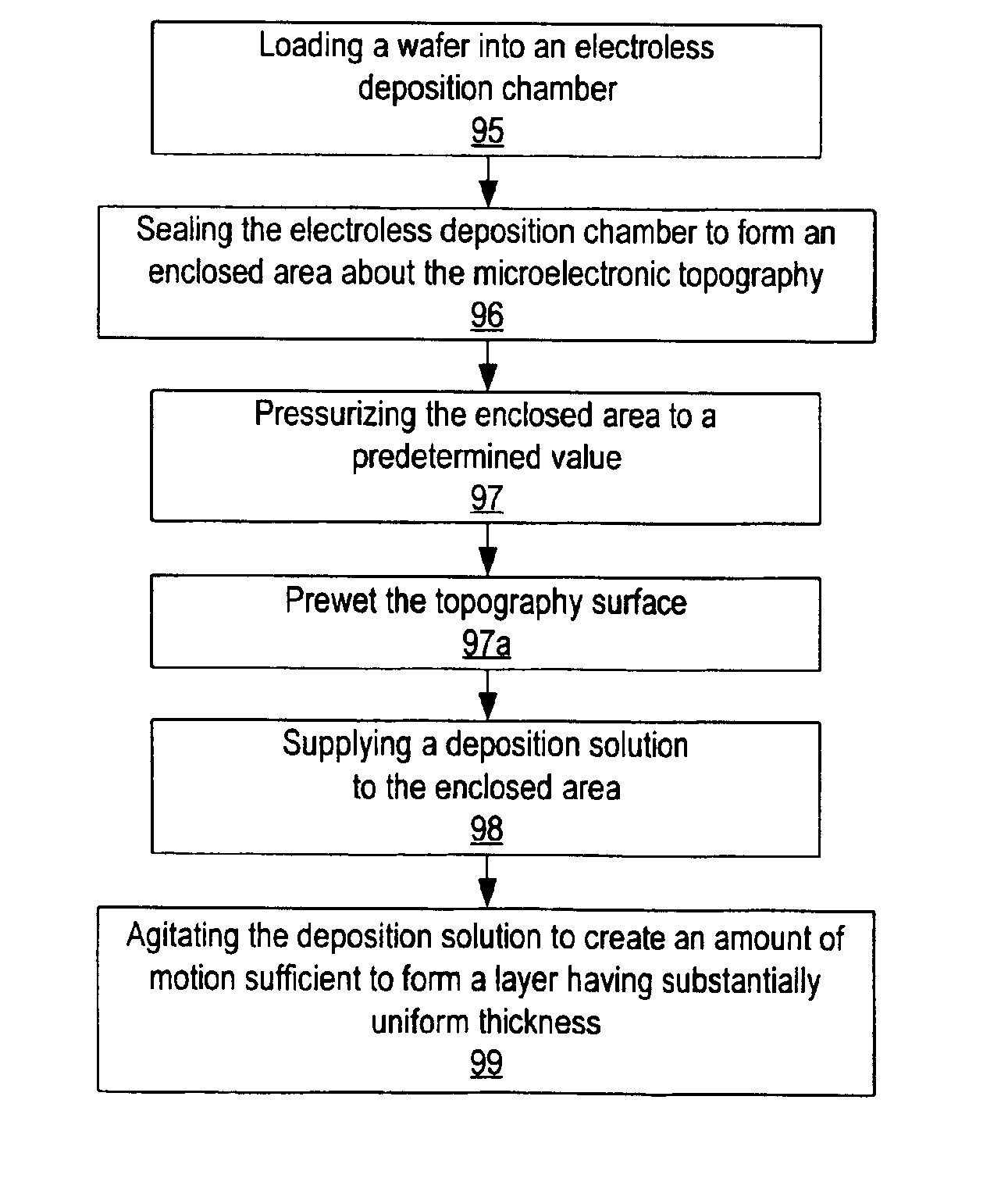
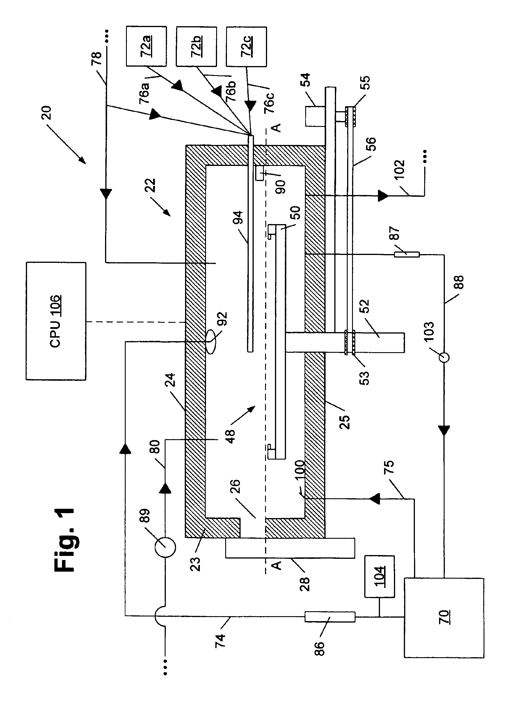
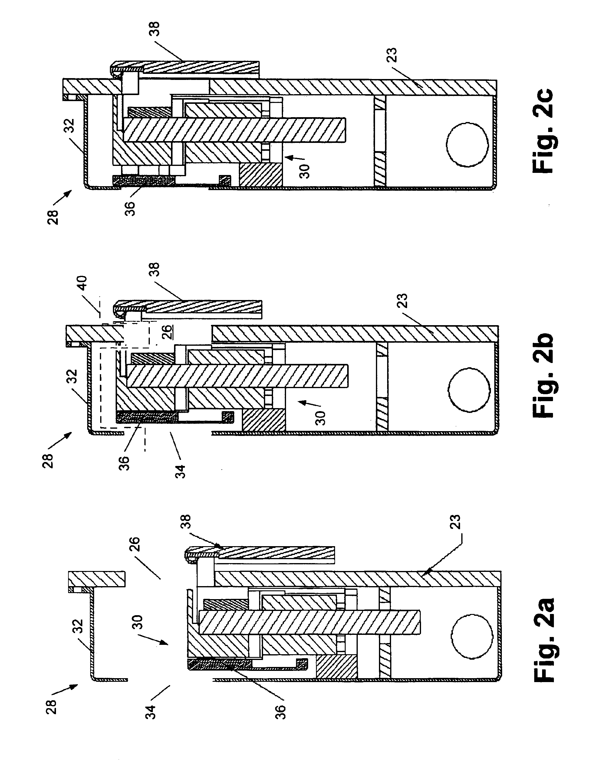
[0068]Turning now to the drawings, exemplary embodiments of systems and methods for processing a microelectronic topography are illustrated in FIGS. 1-18. More specifically, FIG. 1 illustrates an exemplary embodiment of a system that may be used for processing a microelectronic topography, while FIGS. 2a-10 show detailed illustrations of particular components of the system in FIG. 1 as well as methods of using such a system. Furthermore, FIGS. 11-18 illustrate a method for processing a microelectronic topography which may be conducted using the system shown in FIG. 1 or any other system adapted for such a method. It is noted that the plurality of component designs and methods illustrated in FIGS. 1-18 are not co-dependent and, therefore, may not necessarily be employed together. In particular, the system described herein may be constructed to include any combination of the components described in reference to FIGS. 1, 2a-2c, 4, 6a-6d, 8a, 8b, and 9a-9c. In addition, the methods for ...


PUM

PropertyMeasurementUnit
frequencyaaaaaaaaaa
angleaaaaaaaaaa
angleaaaaaaaaaa

Abstract

Methods and systems are provided which are adapted to process a microelectronic topography, particularly in association with an electroless deposition process. In general, the methods may include loading the topography into a chamber, closing the chamber to form an enclosed area, and supplying fluids to the enclosed area. In some embodiments, the fluids may fill the enclosed area. In addition or alternatively, a second enclosed area may be formed about the topography. As such, the provided system may be adapted to form different enclosed areas about a substrate holder. In some cases, the method may include agitating a solution to minimize the accumulation of bubbles upon a wafer during an electroless deposition process. As such, the system provided herein may include a means for agitating a solution in some embodiments. Such a means for agitation may be distinct from the inlet / s used to supply the solution to the chamber.

Description

BACKGROUND OF THE INVENTION[0001]1. Field of the Invention[0002]This invention generally relates to methods and a system for processing a microelectronic topography, particularly for processes associated with an electroless deposition process.[0003]2. Description of the Related Art[0004]The following descriptions and examples are not admitted to be prior art by virtue of their inclusion within this section.[0005]Electroless plating is a process for depositing materials on a catalytic surface from an electrolyte solution without an external source of current. An advantage of an electroless deposition process is that it can be selective, i.e., the material can be deposited only onto areas that demonstrate appropriate chemical properties. In particular, local deposition can be performed onto metals that exhibit an affinity to the material being deposited or onto areas pretreated or pre-activated, e.g., with a catalyst. The material or catalyst applied onto the selected areas is sometim...

Claims


Application Information

Patent Timeline
Patent Type & Authority Patents(United States)
IPC IPC(8): H01L21/687H01L21/00H01L21/67
CPCH01L21/67051H01L21/68728H01L21/6708Y02P80/30
Inventor IVANOV, IGOR C.ZHANG, WEIGUO
Owner LAM RES CORP
Why Eureka
Try Eureka