Gap tuning for surface micromachined structures in an epitaxial reactor

a micromachined structure and epitaxial reactor technology, applied in the field of micromechanical structure manufacturing, can solve the problems of slow etching rate, limited aspect ratio, and limited lithography and etching process limitations, and achieve high layer deposition rate and production rate. high

Inactive Publication Date: 2005-01-20
ROBERT BOSCH GMBH
View PDF12 Cites 119 Cited by
  • Summary
  • Abstract
  • Description
  • Claims
  • Application Information

AI Technical Summary

Benefits of technology

[0008] The precision control of the width of the gaps between the micromechanical elements on a device in the foregoing manner may provide several advantages including: ready compatibility with an epitaxial environment and standard epitaxy equipment; high production rates due to the high layer deposition rates that may be achieved in an epitaxial reactor; and ready adaptability to use of different materials to be deposited on the micromachined device, including monocrystalline silicon, polycrystalline silicon, a SiGe mixture, pure germanium, or silicon carbide. Furthermore, the deposited layers may be in situ doped.

Problems solved by technology

While etching very narrow trenches to obtain desired narrow gaps has been attempted, these methods may require slower etch rates, may be limited in aspect ratio, and may be subject to limitations of the lithography and etching process.
Similarly, germanium has been applied to produce narrow gaps, however, this process may have process compatibility limitations.

Method used


Image

  • Gap tuning for surface micromachined structures in an epitaxial reactor
  • Gap tuning for surface micromachined structures in an epitaxial reactor
  • Gap tuning for surface micromachined structures in an epitaxial reactor

Examples


Embodiment Construction

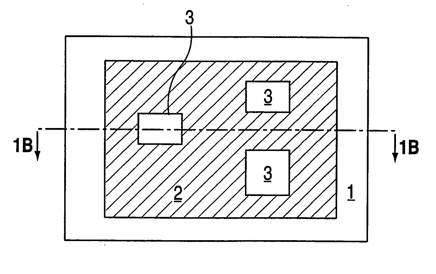
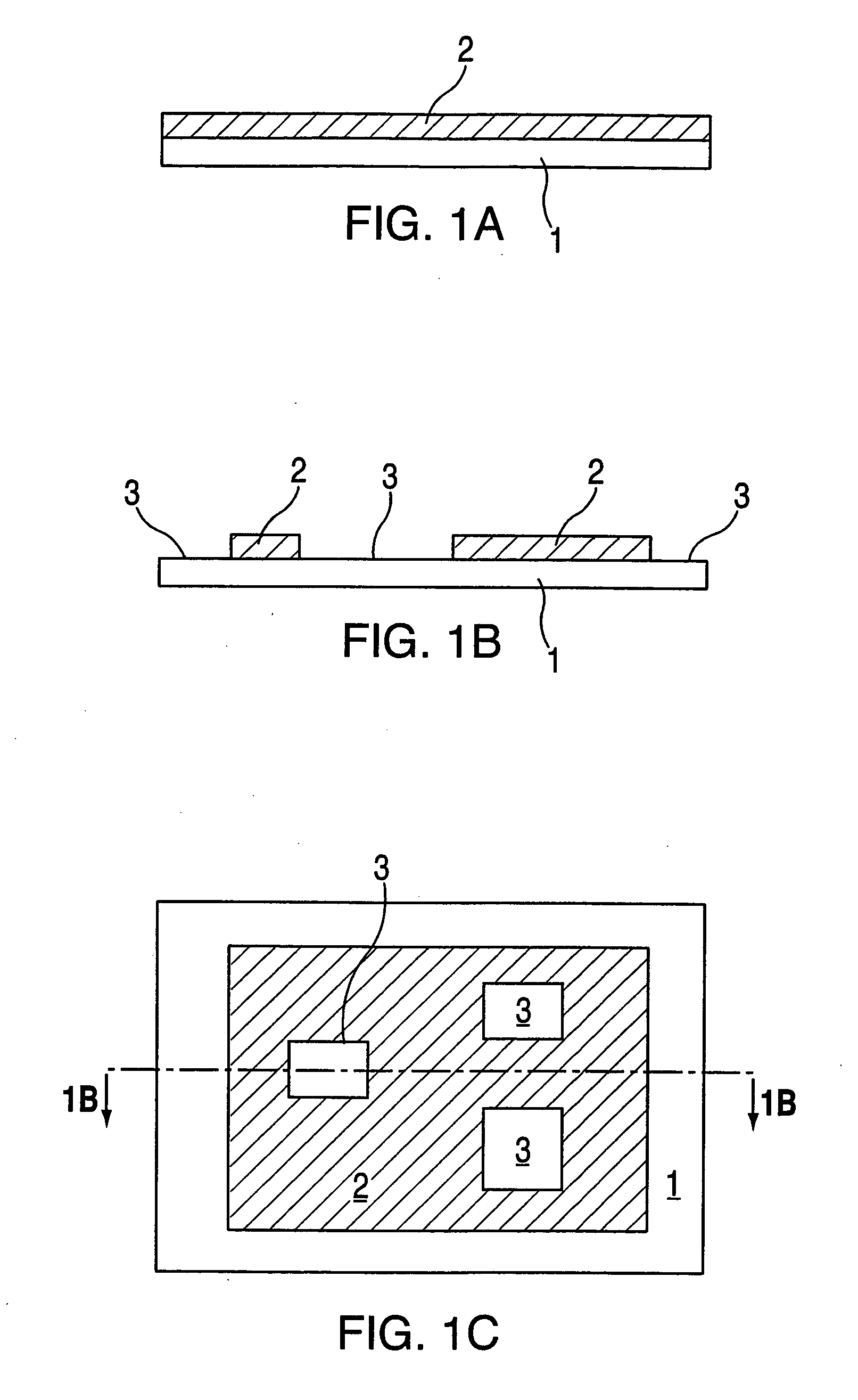
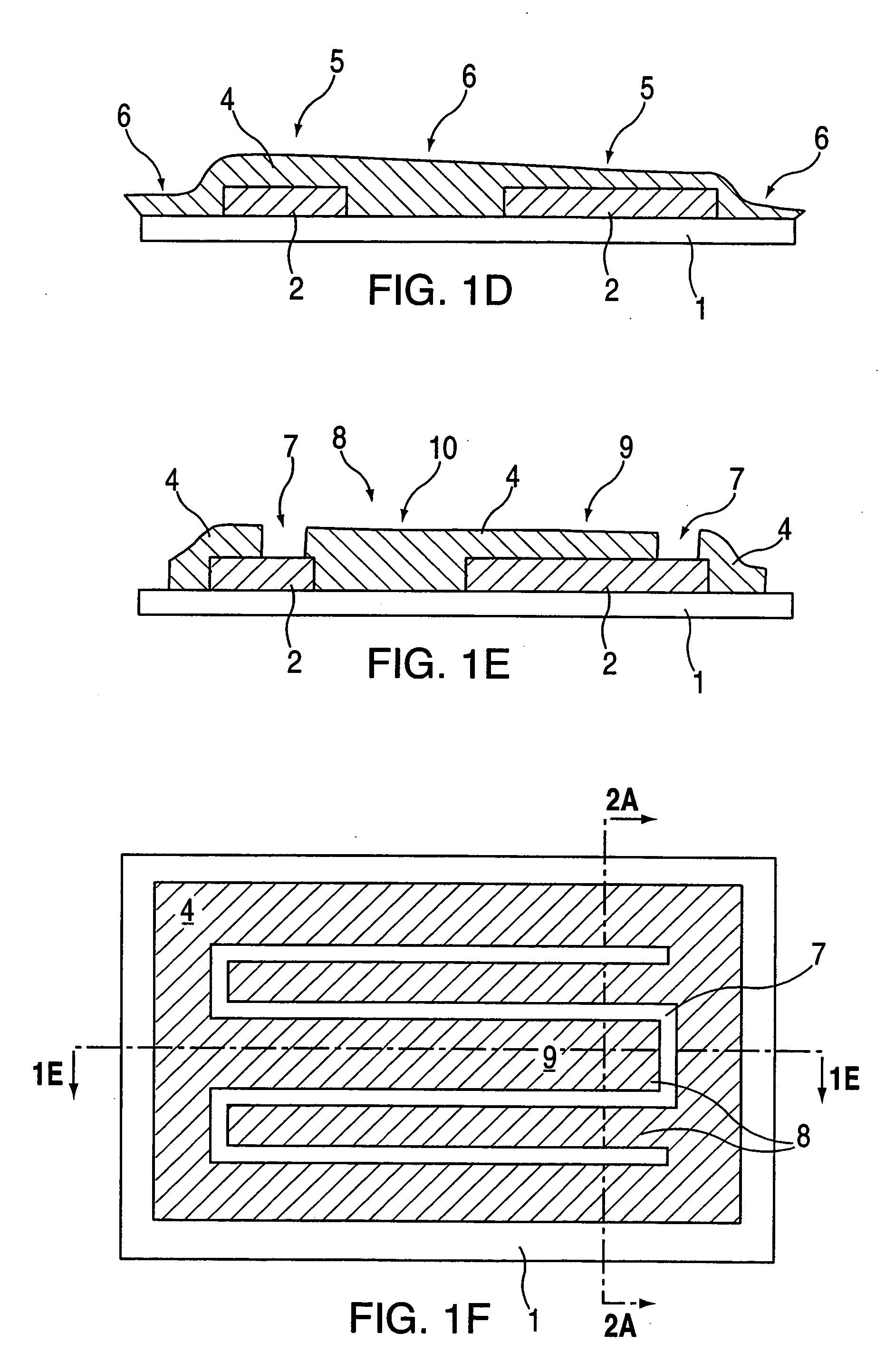
[0015] According to an exemplary embodiment of the present invention, a method for gap tuning a micromachined structure or device is provided. As shown in the cross-section view in FIG. 1a, the partially formed device is based on a substrate layer 1 of, for example, substrate silicon, upon which a sacrificial layer 2 of, for example, SiO2 is deposited in an Low Temperature Oxide (LTO) process or thermally grown. FIG. 1b shows a cross-section view of the substrate / sacrificial layer combination of FIG. 1a after a pattern of holes or open areas 3 have been formed in sacrificial layer 2 using etching techniques, for example by application of a photo-sensitive material over the sacrificial layer, applying a mask with the desired etching pattern over the photo-sensitive material, exposing the masked surface to light, and then applying etchants to remove the exposed portions of the photo-sensitive material then the sacrificial SiO2 underneath the exposed portions. FIG. 1c shows a plan view...


PUM

PropertyMeasurementUnit
thicknessaaaaaaaaaa
temperatureaaaaaaaaaa
pressureaaaaaaaaaa

Abstract

A method for adjusting with high precision the width of gaps between micromachined structures or devices in an epitaxial reactor environment. Providing a partially formed micromechanical device, comprising a substrate layer, a sacrificial layer including silicon dioxide deposited or grown on the substrate and etched to create desired holes and/or trenches through to the substrate layer, and a function layer deposited on the sacrificial layer and the exposed portions of the substrate layer and then etched to define micromechanical structures or devices therein. The etching process exposes the sacrificial layer underlying the removed function layer material. Cleaning residues from the surface of the device, then epitaxially depositing a layer of gap narrowing material selectively on the surfaces of the device. The selection of deposition surfaces determined by choice of materials and the temperature and pressure of the epitaxy carrier gas. The gap narrowing epitaxial deposition continues until a desired gap width is achieved, as determined by, for example, an optical detection arrangement. Following the gap narrowing step, the micromachined structures or devices may be released from their respective underlying sacrificial layer.

Description

FIELD OF THE INVENTION [0001] The present invention relates to manufacture of micromechanical structures, and relates in particular to a method for narrowing a gap between micromachined structures on a device during manufacture in an epitaxial reactor. BACKGROUND INFORMATION [0002] A method of depositing structural layers during manufacture of surface-micromachined devices sometimes involves the use of an epitaxial reactor. Epitaxy is a process for production of layers of monocrystalline layers of silicon over a single crystal substrate, and for forming polycrystalline silicon layers over other substrate materials, for instance SiO2 films on silicon substrates. Epitaxial reactors may be operated with precisely controlled temperature and environmental conditions to ensure uniform deposition and chemical composition of the layer(s) being deposited on the target substrate. In addition to the precise control, use of an epitaxial reactor may permit build-up of layers on a substrate at si...

Claims


Application Information

Patent Timeline
Patent Type & Authority Applications(United States)
IPC IPC(8): B81B3/00B81C1/00B81C99/00
CPCB81B3/0086B81C1/00063B81C2203/0145B81C2203/0136B81C2201/0112
Inventor PARTRIDGE, AARONLUTZ, MARKUS
Owner ROBERT BOSCH GMBH
Why Eureka
Try Eureka