Integrated active devices with improved optical coupling to dielectric waveguides

a dielectric waveguide and active device technology, applied in the field of semiconductor processing, can solve the problems of increasing packaging costs, difficult to provide electrically pumped sources, and introducing scaling limitations, and achieve the effect of facilitating efficient adiabatic transformation

Active Publication Date: 2020-07-23
NEXUS PHOTONICS LLC
View PDF0 Cites 5 Cited by
  • Summary
  • Abstract
  • Description
  • Claims
  • Application Information

AI Technical Summary

Benefits of technology

[0010]In one embodiment, an optical device comprises first, second and third elements fabricated on a common substrate; wherein the first element comprises an active waveguide structure supporting a first optical mode, the second element comprises a passive waveguide structure supporting a second optical mode, and the third element, at least partly butt coupled to the first element, comprises an intermediate waveguide structure. In this embodiment, if the first optical mode differs from the second optical mode by more than a predetermined amount, a tapered waveguide structure in at least one of the second and third elements facilitates efficient adiabatic transformation between the first optical mode and the second optical mode. Mutual alignments of the first, second and third elements are defined using lithographic alignment marks.

Problems solved by technology

The biggest drawback in using silicon for PICs is that it is an indirect bandgap material which makes it hard to provide electrically pumped sources.
Such an approach is challenging due to a need for very fine alignment, which increases packaging costs and introduces scaling limitations.
In cases where there is larger difference in effective indices, such as between e.g. SiN and InP or GaN, the requirements on taper tip dimensions become prohibitive limiting efficient power transfer.
Achieving such dimensions is complex and may be cost prohibitive.
Although InP and silicon-based PICs address many current needs, they have some limitations; among them the fact that the operating wavelength range is limited by material absorption increasing the losses, and the fact that there is a limit on the maximum optical intensities and consequently optimal powers that a PIC can handle.
For comparison, the refractive index of GaAs and InP is >3. This makes the tapered approach challenging.
The alternative hybrid approach suffers from the drawbacks already mentioned above, namely the need for precise alignment, and correspondingly complex packaging and scaling limitations.

Method used


Image

  • Integrated active devices with improved optical coupling to dielectric waveguides
  • Integrated active devices with improved optical coupling to dielectric waveguides
  • Integrated active devices with improved optical coupling to dielectric waveguides

Examples


Embodiment Construction

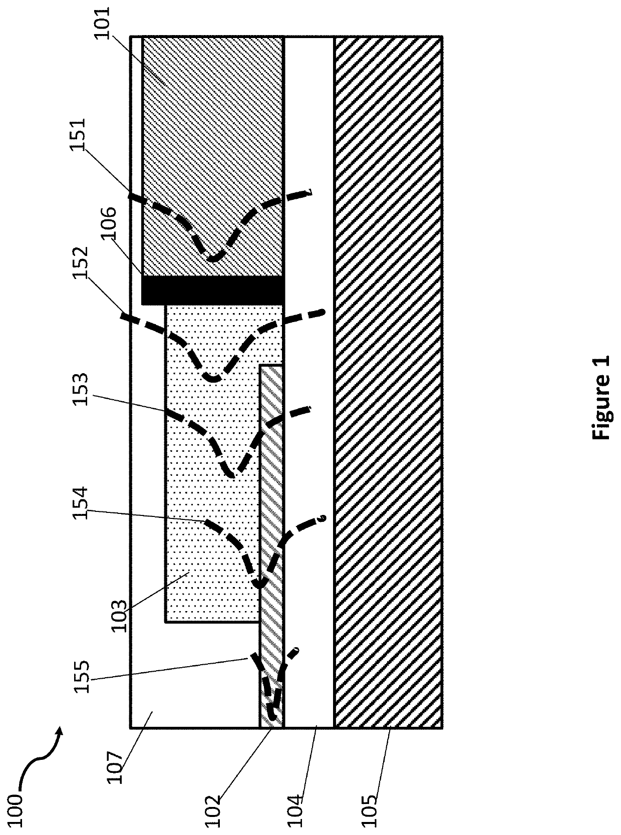
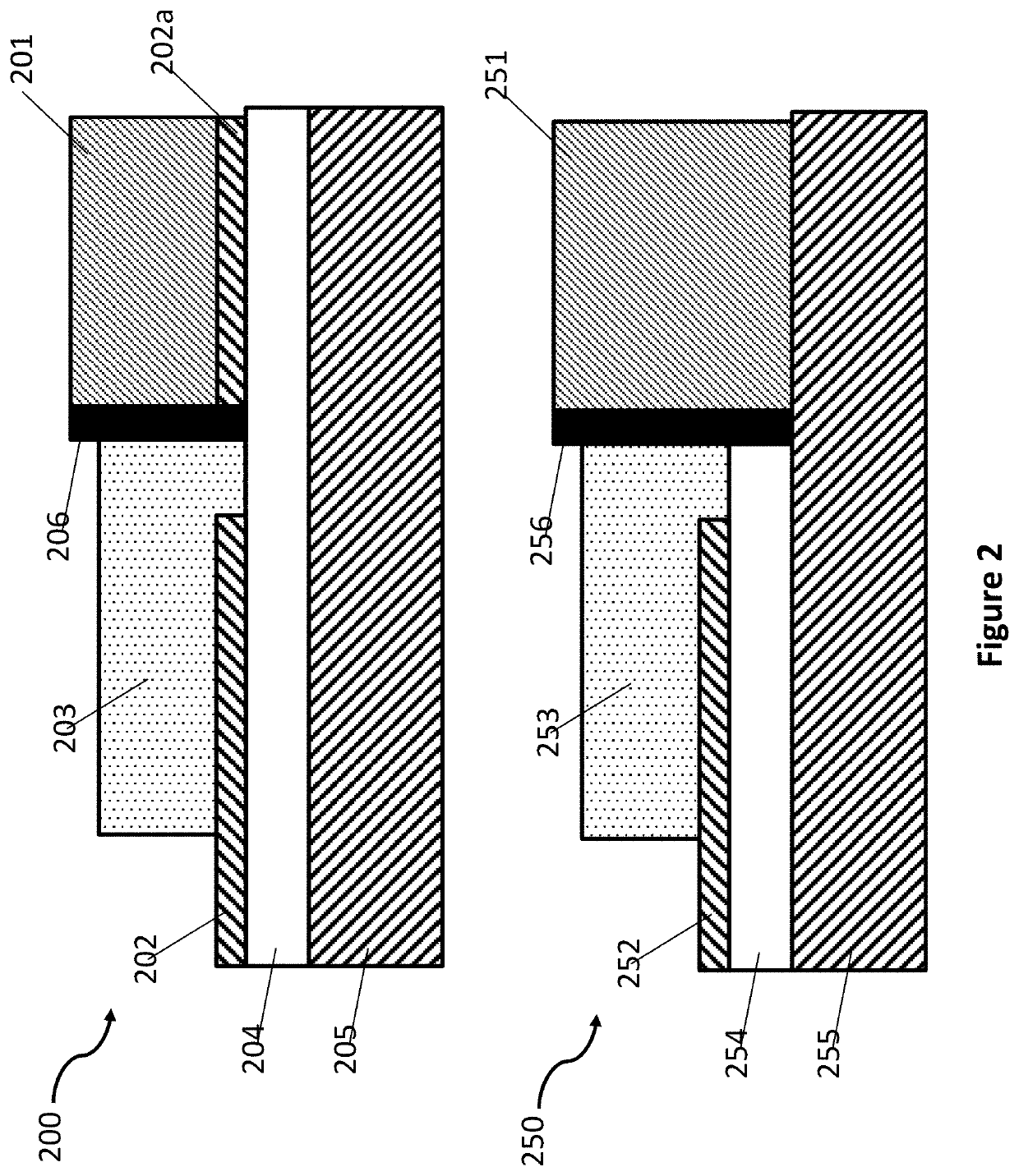
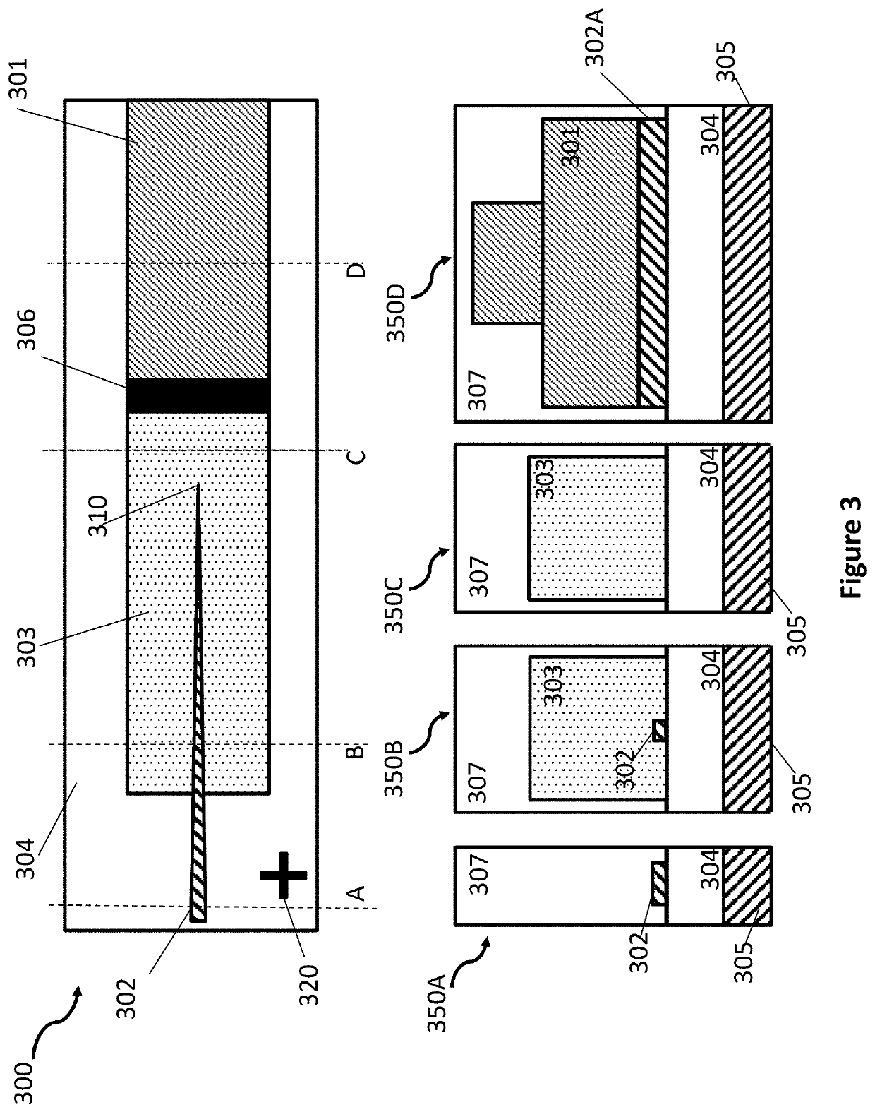
[0019]Described herein include embodiments of a method and system for realization of photonic integrated circuits using wafer bonding and deposition of dissimilar materials where optical coupling is improved by use of mode conversion and a butt-coupling scheme.

[0020]In the following detailed description, reference is made to the accompanying drawings which form a part hereof, wherein like numerals designate like parts throughout, and in which are shown by way of illustration embodiments in which the subject matter of the present disclosure may be practiced. It is to be understood that other embodiments may be utilized and structural or logical changes may be made without departing from the scope of the present disclosure. Therefore, the following detailed description is not to be taken in a limiting sense, and the scope of embodiments is defined by the appended claims and their equivalents.

[0021]The description may use perspective-based descriptions such as top / bottom, in / out, over / ...


PUM

PropertyMeasurementUnit
refractive indicesaaaaaaaaaa
refractive indexaaaaaaaaaa
evanescent fieldaaaaaaaaaa

Abstract

An optical device comprises first, second and third elements fabricated on a common substrate. The first element comprises an active waveguide structure supporting a first optical mode, the second element comprises a passive waveguide structure supporting a second optical mode, and the third element, at least partly butt coupled to the first element, comprises an intermediate waveguide structure. If the first optical mode differs from the second optical mode by more than a predetermined amount, a tapered waveguide structure in at least one of the second and third elements facilitates efficient adiabatic transformation between the first optical mode and the second optical mode. Mutual alignments of the first, second and third elements are defined using lithographic alignment marks.

Description

FIELD OF THE INVENTION[0001]The present invention relates to semiconductor processing. More specifically, certain embodiments of the invention relate to a method and system for realization of photonic integrated circuits using dissimilar materials that are optically coupled.BACKGROUND OF THE INVENTION[0002]A photonic integrated circuit (PIC) or integrated optical circuit is a device that integrates multiple photonic functions and as such is analogous to an electronic integrated circuit. The major difference between the two is that a photonic integrated circuit provides functions for information signals imposed on optical carrier waves. The material platform most commercially utilized for photonic integrated circuits is indium phosphide (InP), which allows for the integration of various optically active and passive functions on the same chip. Although many current PICs are realized in InP platforms, there has been significant research in the past decade in using silicon rather than I...

Claims


Application Information

Patent Timeline
Patent Type & Authority Applications(United States)
IPC IPC(8): G02B6/12G02B6/13G02B6/122
CPCG02B6/1228G02B6/12004G02B6/13G02B2006/12173
Inventor PARK, HYUNDAI
Owner NEXUS PHOTONICS LLC
Why Eureka
Try Eureka