Device for improving image resolution in camera system having lens that permits distortion and operation method thereof

Pending Publication Date: 2022-04-21
SAMSUNG ELECTRONICS CO LTD
View PDF9 Cites 0 Cited by
  • Summary
  • Abstract
  • Description
  • Claims
  • Application Information

AI Technical Summary

Benefits of technology

[0006]Embodiments of the present disclosure provide an electronic device for improving image resolution through re-mosaic processing using

Problems solved by technology

For this reason, it may be more difficult to sec

Method used


Image

  • Device for improving image resolution in camera system having lens that permits distortion and operation method thereof
  • Device for improving image resolution in camera system having lens that permits distortion and operation method thereof
  • Device for improving image resolution in camera system having lens that permits distortion and operation method thereof

Examples


Example

[0025]Below, embodiments of the present disclosure are described in detail such that those skilled in the art may easily implement the described and other embodiments of the present disclosure.

[0026]Components that are described in the detailed description with reference to the terms “unit”, “module”, “block”, or the like, and function blocks illustrated in drawings may be implemented with software, hardware, or a combination thereof. For example, the software may include machine code, firmware, embedded code, application software, or a combination thereof. For example, the hardware may include an electrical circuit, an electronic circuit, a processor, a computer, an integrated circuit, integrated circuit cores, an image sensor, a pressure sensor, an inertial sensor, a microelectromechanical system (MEMS), a passive element, or a combination thereof.

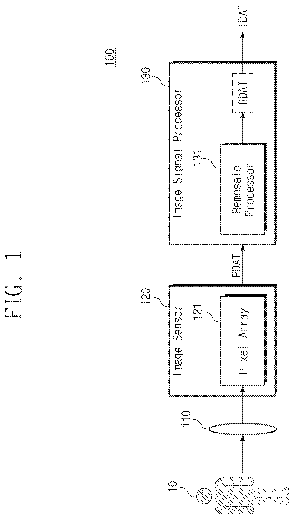
[0027]FIG. 1 illustrates a configuration of an image processing block 100 according to an embodiment of the present disclosure. The ima...


PUM


Abstract

An electronic device, method thereof, and digital camera are provided, including an image sensor that generates pixel data based on light received through a lens that permits distortion where a captured image is compressed in a first direction, and an image signal processor that performs re-mosaic processing on the pixel data for correcting distortion occurring in the first direction and to generate re-mosaiced pixel data.

Description

CROSS-REFERENCE TO RELATED APPLICATIONS[0001]This application claims priority under 35 U.S.C. § 119 to Korean Patent Application No 10-2020-0136546 filed on Oct. 21, 2020, in the Korean Intellectual Property Office, the disclosures of which are incorporated by reference herein in their entireties.FIELD[0002]Embodiments of the present disclosure described herein relate to electronic devices, and more particularly, relate to an electronic device for improving image resolution in a camera system including a lens that permits distortion, and an operation method thereof.DISCUSSION OF RELATED ART[0003]An image sensor may be classified as a charge coupled device (CCD) image sensor, a complementary metal-oxide semiconductor (CMOS) image sensor (CIS), or the like. A CMOS image sensor includes pixels implemented with CMOS transistors, and converts light energy to an electrical signal by using a photoelectric conversion element included in each pixel. The CMOS image sensor obtains information ...

Claims


Application Information

Patent Timeline
IPC IPC(8): G06T3/40G06T5/00H04N5/232
CPCG06T3/4015H04N5/23229G06T5/006H04N5/262H04N23/80H04N25/77H04N25/75G06T2207/10024H04N23/10H04N23/54H04N23/55H04N25/59H04N25/13H04N25/76H04N23/84H04N23/815H04N25/134H04N25/778
Inventor LEE, JEONGGUKCHOI, YUNSEOK
Owner SAMSUNG ELECTRONICS CO LTD
Why Eureka
Try Eureka