
Lens camera module and a camera

A camera module and lens technology, applied in image communication, TV, color TV components and other directions, can solve problems such as easy occurrence of stains, and achieve the effect of improving image resolution, strong reliability, and simple structure

Inactive Publication Date: 2019-05-28
TRULY OPTO ELECTRONICS
View PDF5 Cites 0 Cited by
  • Summary
  • Abstract
  • Description
  • Claims
  • Application Information

AI Technical Summary

Problems solved by technology

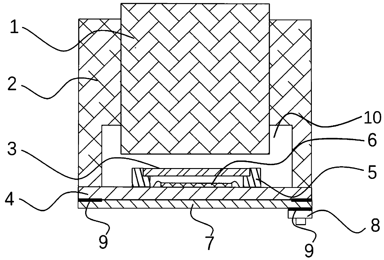
[0004] The purpose of the present invention is to address the deficiencies in the above technologies, and propose a lens camera module and camera, aiming to solve the problem that the existing CSP lens is prone to stains when used in conjunction with the COB Sensor (image sensor)

Method used


Image

  • Lens camera module and a camera

Examples


Embodiment Construction

[0019] It should be noted that, in the case of no conflict, the embodiments in the present application and the features in the embodiments can be combined with each other. The present invention will be described in detail below with reference to the accompanying drawings and examples.

[0020] In describing the present invention, it should be understood that the terms "center", "longitudinal", "transverse", "length", "width", "thickness", "upper", "lower", "front", " Back", "Left", "Right", "Vertical", "Horizontal", "Top", "Bottom", "Inner", "Outer", "Clockwise", "Counterclockwise", "Axial", The orientation or positional relationship indicated by "radial", "circumferential", etc. is based on the orientation or positional relationship shown in the drawings, and is only for the convenience of describing the present invention and simplifying the description, rather than indicating or implying the referred device or element Must be in a particular orientation, be constructed in a...


PUM


Abstract

The invention provides a lens camera module and a camera. The lens camera module comprises a CSP lens and a lens base. The CSP lens is connected to the upper end of the lens base; The bottom of the lens base is connected with a PCB substrate; A COB Sensor (image sensor) is arranged on the PCB substrate; An independent small base is arranged on the PCB substrate; Protective glass is mounted on theindependent small base; The protective glass is positioned above the COB image sensor; The protective glass is used for preventing stains from entering the COB image sensor; According to the scheme provided by the invention, the problem that stains are easy to appear when the CSP lens is matched with the COB image sensor is avoided, the resolving power of the lens is improved, the structure is simple, the reliability is high, and the method is suitable for cameras, mobile phone lenses and the like.

Description

technical field [0001] The invention belongs to the technical field of lens module packaging, and in particular relates to a lens camera module and a camera. Background technique [0002] With the continuous advancement of technology, users' requirements for cameras are constantly improving; the photosensitive chips and circuit boards of existing cameras generally adopt chip-scale packaging (Chip Scale Package, referred to as: CSP); however, with the application of image sensing With the continuous development of the industry, the packaging form is also constantly changing; from CSP packaging to chip on board packaging (Chip On Board, referred to as: COB), chip on board packaging (Chip On Board, referred to as: COB) has gradually become the mainstream; at the same time, CSP lens The package combined with COBSensor (image sensor) is also favored by users. [0003] Conventional large-size CSP lens mainly faces two problems when used with COB Sensor (image sensor). One is that...

Claims


Application Information

Patent Timeline
IPC IPC(8): H04N5/225
Inventor 梁晓龙
Owner TRULY OPTO ELECTRONICS
Learn More