Semiconductor memory device and electronic device

a memory device and semiconductor technology, applied in the field of active control of word lines, can solve the problems of shortening the time elapsed before the start of a read access, and achieve the effect of removing the long rate restriction of a semiconductor memory devi

a memory device and semiconductor technology, applied in the field of active control of word lines, can solve the problems of shortening the time elapsed before the start of a read access, and achieve the effect of removing the long rate restriction of a semiconductor memory devi

US6925023B2Inactive Publication Date: 2005-08-02SEIKO EPSON CORP

Image

  • Semiconductor memory device and electronic device
  • Semiconductor memory device and electronic device
  • Semiconductor memory device and electronic device

Examples


Embodiment Construction

[0035]One mode of carrying out the invention is discussed below as a preferred embodiment in the following sequence:

A. Terminal Structure of Semiconductor Memory Device and Outline of Working State

B. Internal Structure of Semiconductor Memory Device

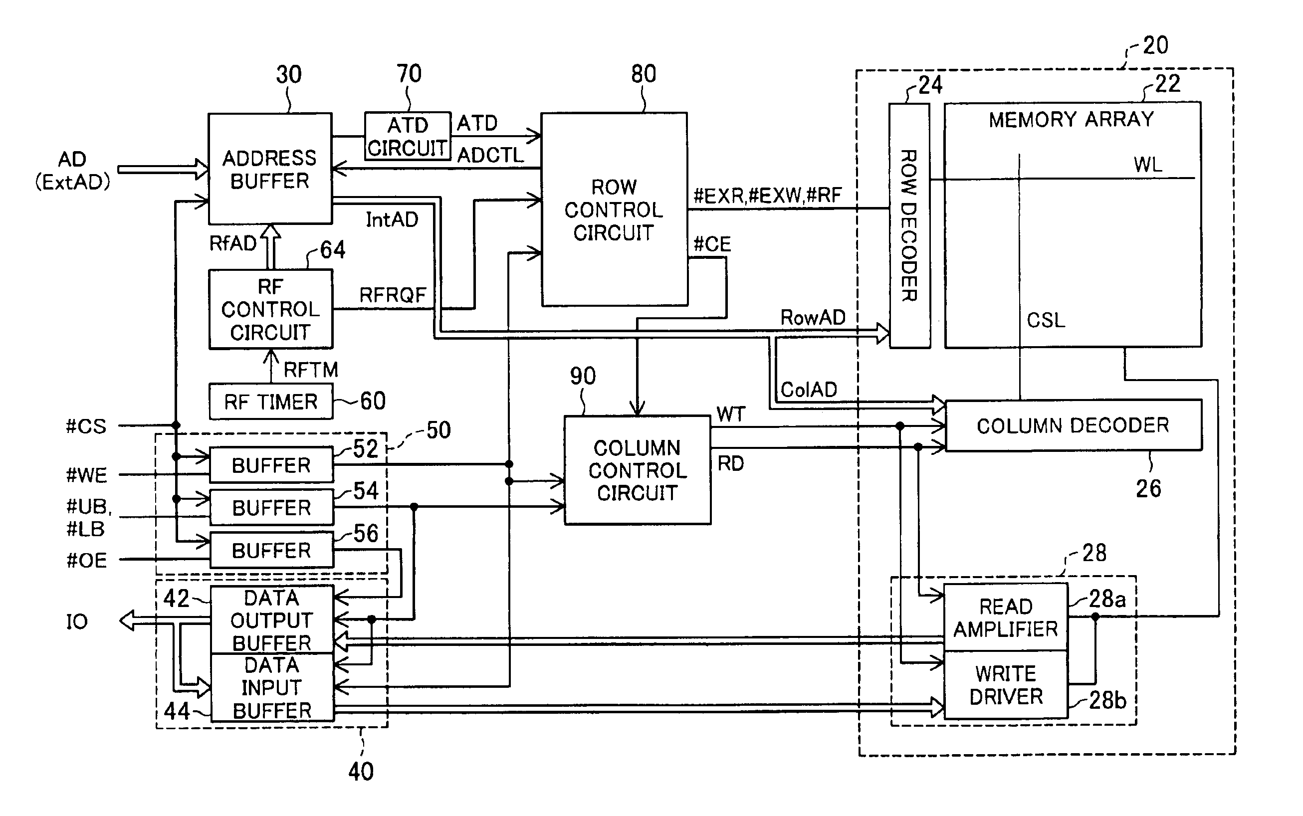
[0036]B1. General Structure

[0037]B2. Row Control Circuit[0038]B.2.1 Read Execution Signal Generator[0039]B.2.2 Write Execution Signal Generator[0040]B.2.3 Refresh Execution Signal Generator[0041]B.2.4 Operations of Respective Generators

[0042]B3. Address Buffer and Data Input Buffer[0043]B.3.1 Address Buffer[0044]B.3.2 Data Input Buffer

C. Operations in Operation Mode

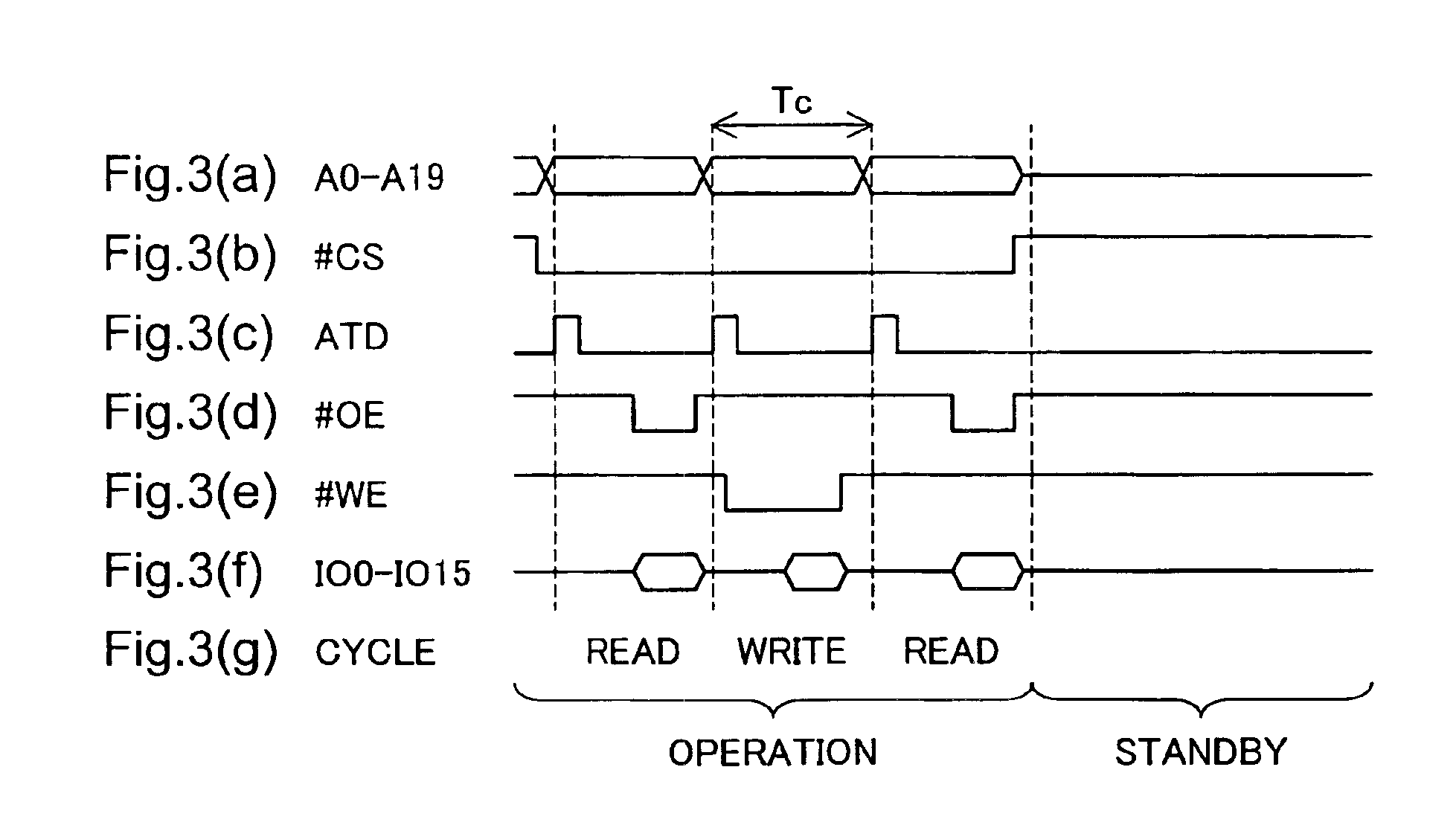
[0045]C1. Read Access

[0046]C2. Early Write Access

[0047]C3. Delay Write Access

D. Application to Electronic Device

A. Terminal Structure of Semiconductor Memory Device and Outline of Working State

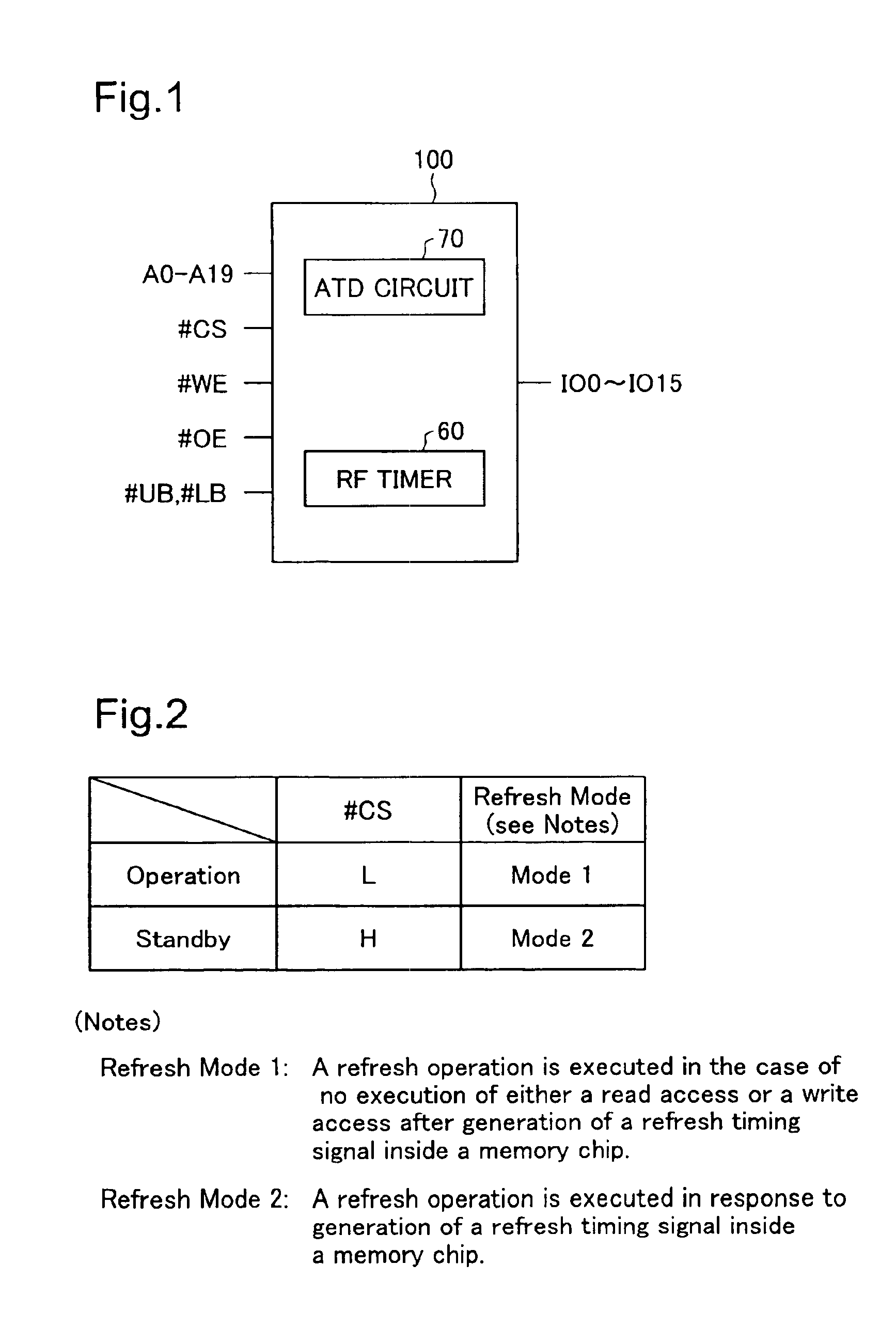
[0048]FIG. 1 shows the terminal structure of a memory chip 100 in one embodiment of the semiconductor memory device of the invention. The memory chip 100 has terminals given below:[0049]A...


PUM


Abstract

In the semiconductor memory device of the invention, while a write enable signal supplied from an external device is at an active level representing a data writing request, an access control module prohibits start of any of a read access operation, a write access operation, and a refresh operation, even in the case of generation of any one of a read access request, a write access request, and a refresh request. Even in the case of generation of a write access request or a refresh request in advance, the access control module preferentially executes a read access operation in response to a read access request generated by a change of an external access timing signal to an inactive level while the write enable signal is at an inactive level. This arrangement desirably eliminates the long rate restriction of the semiconductor memory device.

Description

BACKGROUND OF THE INVENTION[0001]1. Field of the Invention[0002]The present invention relates to activation control of word lines in a semiconductor memory device having a memory array, in which dynamic memory cells are arranged in a matrix.[0003]2. Description of the Related Art[0004]Typically used semiconductor memory devices are DRAMs and SRAMs. As is well known in the art, the DRAM is more moderately priced and has the larger capacity than the SRAM but requires refresh operations. The SRAM does not conveniently require refresh operations, but is more expensive and has the smaller capacity than the DRAM.[0005]A known virtual SRAM (VSRAM: Virtually Static RAM) has been developed as the semiconductor memory device having the advantages of both the DRAM and the SRAM. The virtual SRAM (also called pseudo SRAM (PSRAM: Pseudo Static RAM)) has a memory cell array of dynamic memory cells like the DRAM and a built-in refresh timer to internally execute refresh operations. An external devi...

Claims


Application Information

Patent Timeline
02 Aug 2005
Publication
US6925023B2
IPC
G11C11/406; G11C11/403
CPC
G11C11/406; G11C11/40603; G11C11/40615
Inventors
MIZUGAKI, KOICHI; OTSUKA, EITARO