Method of manufacturing a semiconductor light-emitting element

a technology of semiconductor light-emitting elements and manufacturing methods, which is applied in the direction of basic electric elements, semiconductor devices, electrical equipment, etc., can solve the problems of affecting the light-emitting diode's luminance, affecting the light-emitting element's probability of light being emitted,

Inactive Publication Date: 2006-05-02
KK TOSHIBA
View PDF8 Cites 147 Cited by
  • Summary
  • Abstract
  • Description
  • Claims
  • Application Information

AI Technical Summary

Benefits of technology

[0018]eliminating one of the phases of the diblock copolymer that has been phase-separated to form a mask material layer having a pattern constituted by the other phase; and

Problems solved by technology

Light having a larger incidence angle than this critical angle is totally reflected, thus greatly degrading the probability of the light being emitted from the light-emitting element.
These methods are however accompanied by the problem that due to the influence of the crystallinity of the substrate, the roughening of the surface of the current diffusion layer may become impossible depending on the orientation of the surface being exposed.
Therefore, roughening of the surface of the chip may not necessarily be possible, so that, the extraction efficiency of the light is prevented from being improved, thus making it difficult to enhance the luminance of the light-emitting diode.
As described above, the conventional light-emitting diode packaged by resin is accompanied by the problem that the incident light to be entered obliquely into the interface between the uppermost layer of the semiconductor multi-layer including a light-emitting layer and a transparent resin is totally reflect from the interface, thus degrading the light extraction efficiency of the light.

Method used


Image

  • Method of manufacturing a semiconductor light-emitting element
  • Method of manufacturing a semiconductor light-emitting element
  • Method of manufacturing a semiconductor light-emitting element

Examples


first embodiment

(First Embodiment)

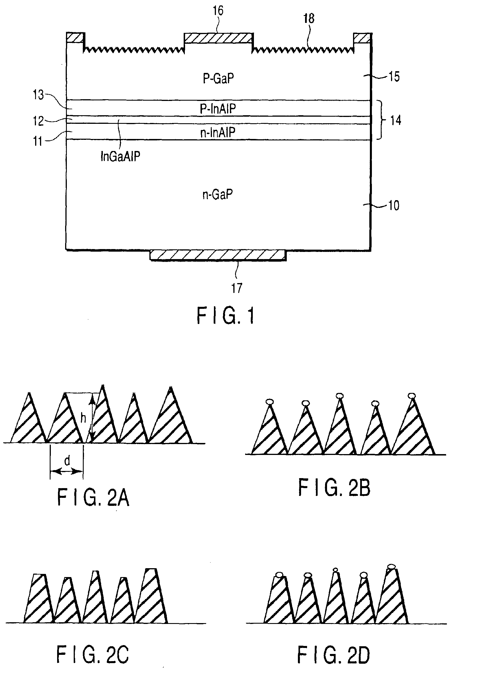
[0032]FIG. 1 is a cross-sectional view illustrating the element structure of an LED according to a first embodiment of the present invention.

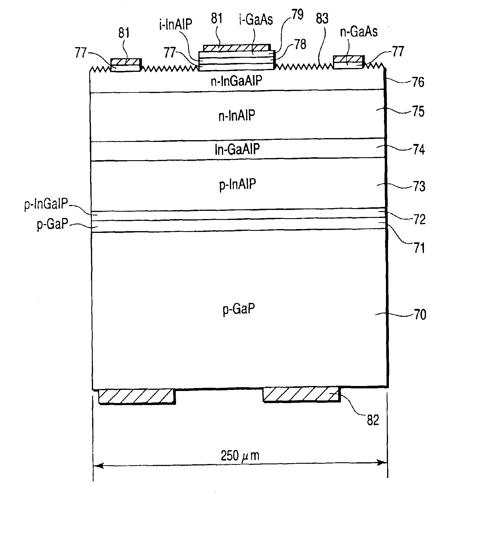
[0033]As shown in FIG. 1, on the top surface (the first surface) of an n-type GaP substrate 10 are deposited semiconductor laminated layers comprising a hetero structure portion 14 which is constituted by an n-type InAlP clad layer 11, an InGaAlP activated layer 12 and a p-type InAlP clad layer 13; and a p-type GaP current diffusion layer 15. A p-side electrode (upper electrode) 16 is formed on part of the surface of the current diffusion layer 15 with the remaining portion of the surface of the current diffusion layer 15 being left exposed. On the other hand, an n-side electrode (lower electrode) 17 is formed on the bottom surface (the second surface) of the substrate 10. The light emitted from the activated layer 12 is taken up from the exposed surface of the current diffusion layer 15. Namely, the exposed surface of the cur...

second embodiment

(Second Embodiment)

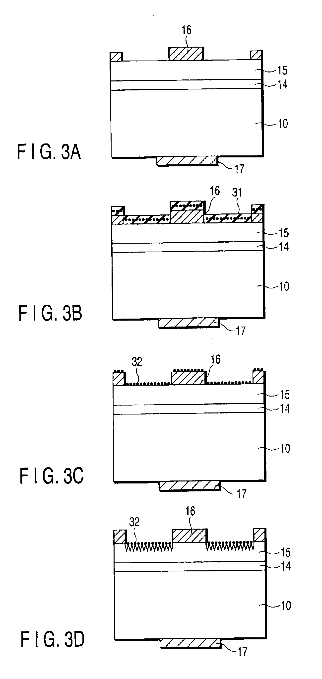
[0048]A PS pattern was formed by RIE under the same conditions as described in the aforementioned first embodiment except that O2 was substituted for CF4.

[0049]In the same manner as described in the first embodiment, a polymer layer 31 containing a diblock copolymer was formed on the surface of the current diffusion layer 15 and then, the diblock copolymer was subjected to phase separation. Then, the polymer layer 31 was subjected to etching by RIE using O2 gas (30 sccm) under the conditions of 13.3 Pa in pressure and 100 W in power output. In contrast with the etching using CF4, although it was impossible, in this case where O2 was employed, to etch the polymer layer 31 down to the underlying substrate, it was possible to relatively accurately remove the PMMA phase of the PS-PMMA block, thereby forming a PS pattern.

[0050]This PS pattern was then transcribed onto the surface of the current diffusion layer 15 by RIE under the same conditions as described in the afo...

third embodiment

(Third Embodiment)

[0052]In this embodiment, a PS pattern was formed through the scission of the main chain of polymer by the irradiation of electron beam.

[0053]In the same manner as described in the first embodiment, a polymer layer 31 containing a diblock copolymer was formed on the surface of the current diffusion layer 15 and then, the diblock copolymer was subjected to phase separation. Then, an electron beam was irradiated the entire surface of the polymer layer 31 to cut the main chain of PMMA. On this occasion, the conditions of irradiating the electron beam were set to 2 eV. Thereafter, the polymer layer 31 was subjected to development by using a developing solution (for example, a mixed solution comprising MIBK (methylisobutyl ketone) and IPA(isopropanol)). The resultant surface of the polymer layer 31 was then rinsed by IPA or ethanol to selectively dissolve and remove the PMMA, thereby leaving a pattern 32 of PS.

[0054]This PS pattern was then transcribed onto the surface ...


PUM


Abstract

There is disclosed a semiconductor light-emitting element comprising a substrate having a first surface and a second surface, a semiconductor laminate formed on the first surface of the substrate and containing a light-emitting layer and a current diffusion layer having a light-extracting surface. The light-emitting element is provided with a light-extracting surface which is constituted by a finely recessed / projected surface, 90% of which is constructed such that the height of the projected portion thereof having a cone-like configuration is 100 nm or more, and the width of the base of the projected portion is within the range of 10-500 nm.

Description

CROSS-REFERENCE TO RELATED APPLICATIONS[0001]This application is based upon and claims the benefit of priority from the prior Japanese Patent Applications No. 2002-010571, filed Jan. 18, 2002, the entire contents of which are incorporated herein by reference.BACKGROUND OF THE INVENTION[0002]1. Field of the Invention[0003]The present invention relates to a semiconductor light-emitting element such as a light-emitting diode (LED), a semiconductor laser (LD), etc., and to a method of manufacturing the semiconductor light-emitting element.[0004]2. Description of the Related Art[0005]A light-emitting diode of high luminance is conventionally constructed such that a light-emitting portion constituted by a double-hetero structure, etc., is disposed on the surface of a semiconductor substrate, and a current diffusion layer is deposited on the light-emitting portion. As this light-emitting diode is packaged by resin, the upper portion of the current diffusion layer is covered with a transpar...

Claims


Application Information

Patent Timeline
Patent Type & Authority Patents(United States)
IPC IPC(8): H01L21/00H01L33/06H01L21/302H01L33/14H01L33/22H01L33/32
CPCH01L33/22
Inventor SUGIYAMA, HITOSHIOHASHI, KENICHIYAMASHITA, ATSUKOWASHIZUKA, SHOICHIAKAIKE, YASUHIKOYOSHITAKE, SHUNJIASAKAWA, KOJIEGASHIRA, KATSUMIFUJIMOTO, AKIRA
Owner KK TOSHIBA
Why Eureka
Try Eureka