
Semiconductor integrated circuit

a technology of integrated circuits and semiconductors, applied in the direction of differential amplifiers, amplifiers with semiconductor devices/discharge tubes, instruments, etc., can solve the problems of amplifier power consumption increasing, distortion of sr enhancement,

Inactive Publication Date: 2006-06-06
KK TOSHIBA
View PDF4 Cites 22 Cited by
  • Summary
  • Abstract
  • Description
  • Claims
  • Application Information

AI Technical Summary

Problems solved by technology

However, the SR Enhancement has a problem of distorting a signal waveform generated at end of the falling edge.
A Class-C amplifier switches off at the falling edge of an output signal, and the above problem is occurred because a driving force of an amplifier declines rapidly.
As a result a power consumption of the amplifier becomes large.
This is a serious problem for example, in a portable apparatus for which low power consumption operation is needed.

Method used


Image

  • Semiconductor integrated circuit
  • Semiconductor integrated circuit
  • Semiconductor integrated circuit

Examples


first embodiment

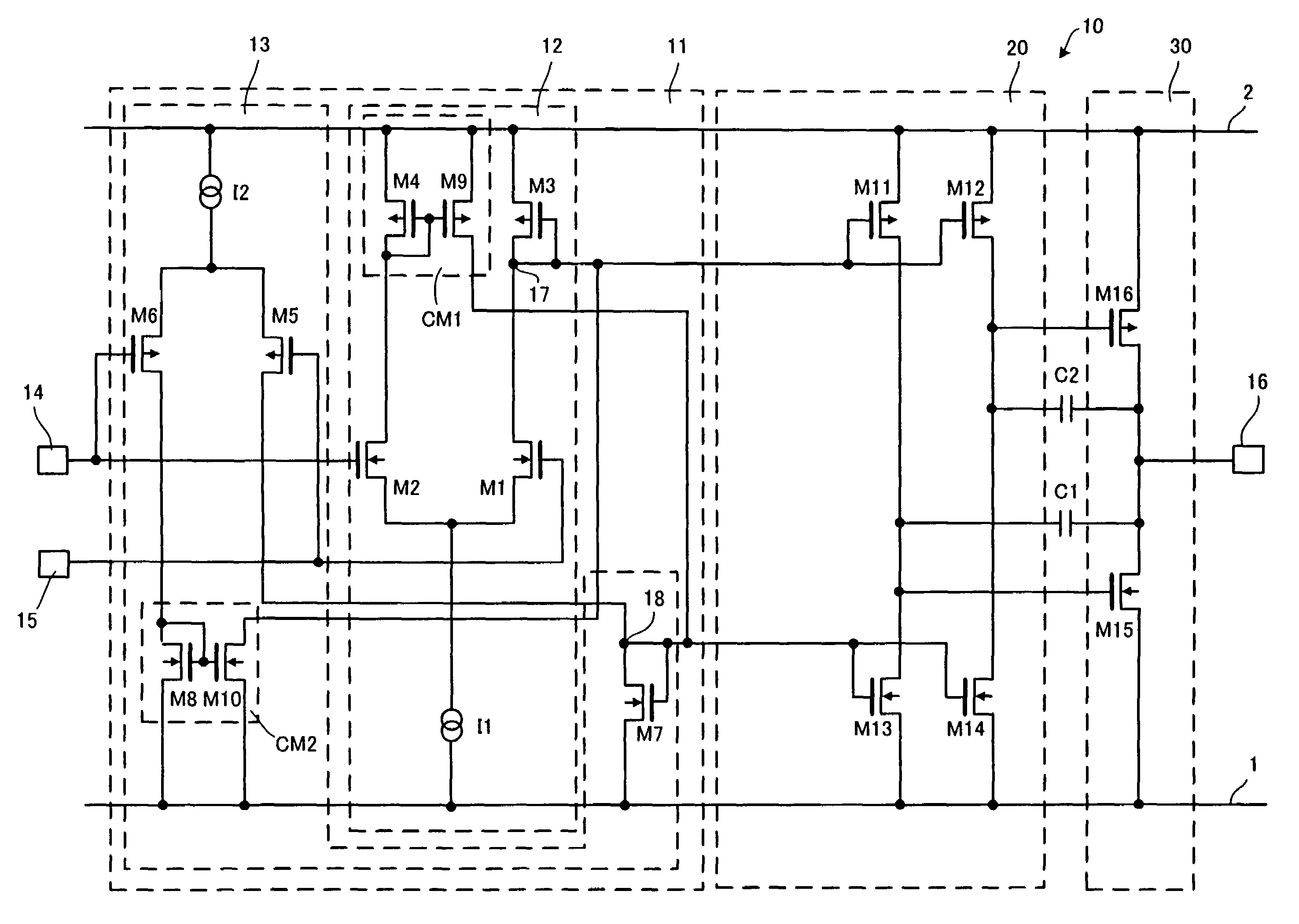
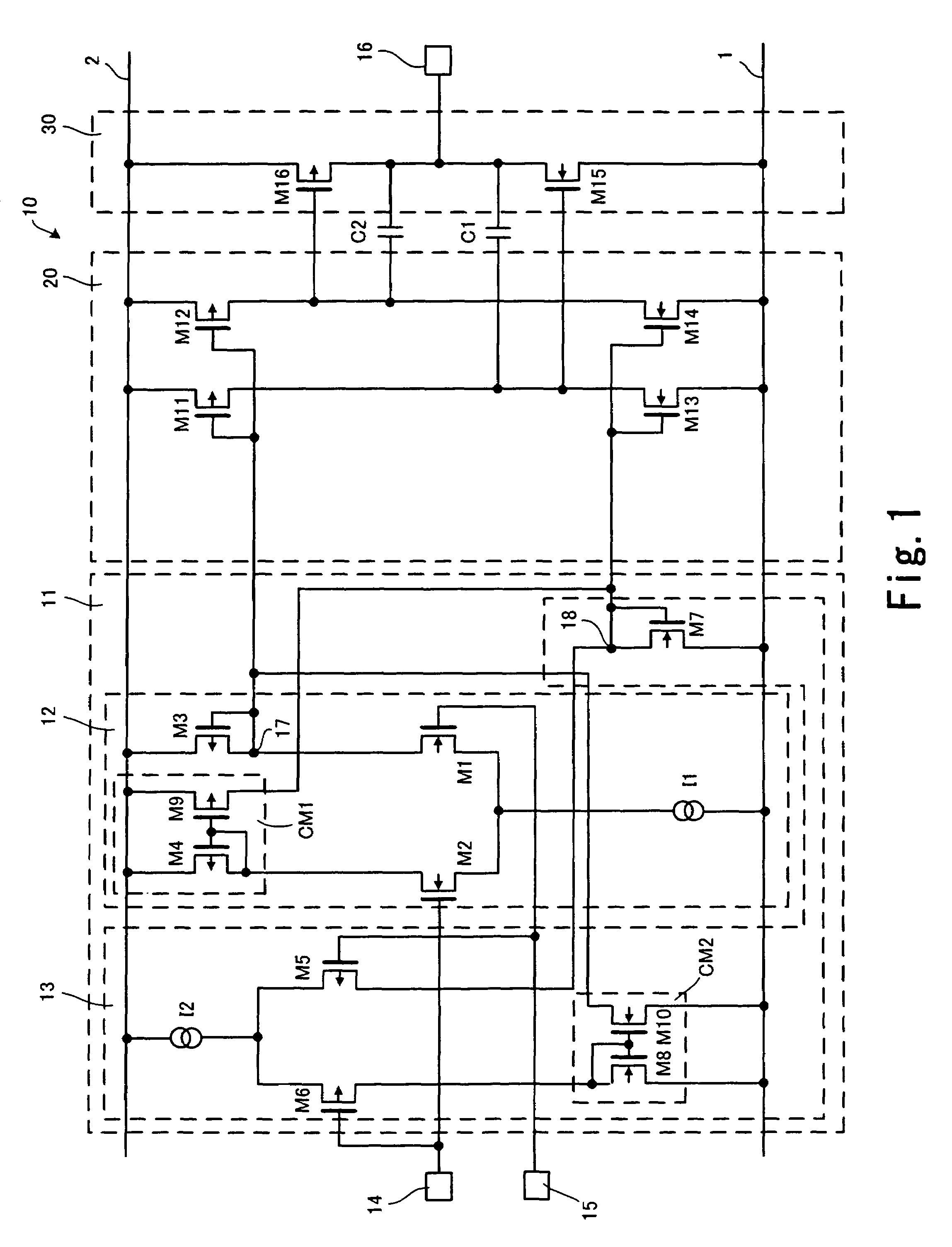
[0017]FIG. 1 is a circuit diagram of a semiconductor integrated circuit including an output amplifier concerning a first embodiment in accordance with the present invention.

[0018]Output amplifier 10 includes two input terminals (positive input terminal 14, negative input terminal 15), output terminal 16, differential amplification circuit 11, output stage control circuit 20, and output stage 30.

[0019]Differential amplification circuit 11 includes N type differential amplification circuit 12 having n channel transistors forming an input stage, and P type differential amplification circuit 13 having p channel transistors.

[0020]If first power supply 1 is set to 0V and second power supply 2 is set to 5V, N type differential amplification circuit 12 carries out differential amplification operation within the range of 1V to 5V, and P type differential amplification circuit 13 carries out differential amplification operation within the range of 0V to 4V. Therefore, it can amplify Rail to R...

second embodiment

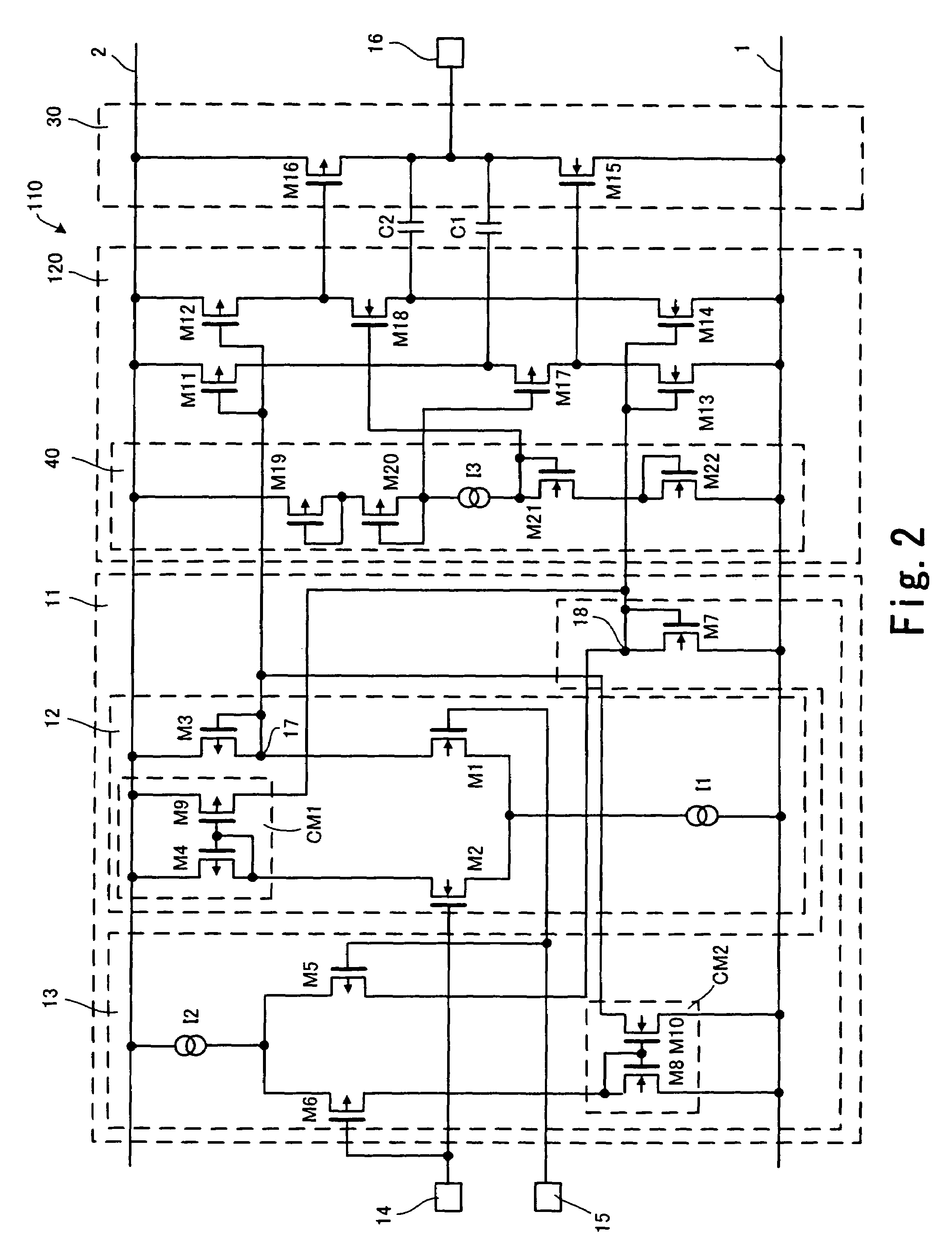
[0055]FIG. 2 shows a circuit diagram of a semiconductor integrated circuit including an output amplifier, in accordance with the present invention.

[0056]In the second embodiment, similar to the first embodiment described above, output amplifier 10 includes two input terminals (positive input terminal 14, negative input terminal 15), output terminal 16, differential amplification circuit 11, and output stage 30. And output amplifier 10 also includes output stage control circuit 120.

[0057]Since a structure of differential amplification circuit 11, first and second current mirror circuits CM1 and CM2 shown in FIG. 2 are the same as those of the first embodiment shown in FIG. 1, explanation of these parts is omitted.

[0058]In the embodiment shown in FIG. 2, output stage control circuit 120 has three p type MOS transistors M11, M12, and M17, three n type MOS transistors M13, M14, and M18, and gate voltage control circuit 40.

[0059]Both gate electrodes of p type MOS transistors M11 and M12 ...

third embodiment

[0107]FIG. 3 is a circuit diagram of a semiconductor integrated circuit including an output amplifier according to a

[0108]Output amplifier 210 of the third embodiment includes two input terminals (positive input terminal 14, negative input terminal 15), output terminal 16, differential amplification circuit 211, output stage control circuit 220, and output stage 30.

[0109]Since a structure of gate voltage control circuit 40, first and second current mirror circuits CM1 and CM2 shown in FIG. 3 are the same as those of the second embodiment shown in FIG. 2, detailed explanation of these parts is omitted.

[0110]Differential amplification circuit 211 of this embodiment includes N type differential amplification circuit 212 and P type differential amplification circuit 213. Although, as for N type differential amplification circuit 212, n type MOS transistor M7 is connected to first power supply 1 through resistance R2 unlike N type differential amplification circuit 12 of the second embod...


PUM


Abstract

A semiconductor integrated circuit includes first and second differential amplification devices to amplify a voltage difference of input signals inputted from a positive input terminal and a negative input terminal, first and second addition devices to add an output of the first differential amplification device and the output of the second differential amplification device, an output stage control device controlled by the first and second addition devices, and output stage controlled by the output stage control device, and an output terminal connected to the output stage.

Description

CROSS REFERENCE TO RELATED APPLICATION[0001]This patent application claims the benefit of priority from Japanese Patent Application No. 2004-172157, filed on Jun. 10, 2004; the content of which is incorporated herein by reference in its entirety.FIELD OF THE INVENTION[0002]This invention relates to a semiconductor integrated circuit including an output amplifier.DESCRIPTION OF THE BACKGROUND[0003]Displaying an LCD (Liquid Crystal Display) is controlled by an LCD driver. An output stage of the driver has an output amplifier for an output signal. It is often suitable to use a Rail-to-Rail amplifier whose output amplitude swings fully in the power supply voltage range as the output amplifier.[0004]U.S. Pat. No. 5,311,145 issued May 10, 1994 describes a circuit of an amplifier which performs Rail-to-Rail operation including a differential amplifier.[0005]In addition, since high-speed operation is also required of an LCD driver, an amplifier having a high Slew Rate (SR) is needed.[0006]A...

Claims


Application Information

Patent Timeline
Patent Type & Authority Patents(United States)
IPC IPC(8): H03F3/45G09G3/36
CPCH03F3/4521G09G3/36H03F3/45
Inventor UENO, MASAJI
Owner KK TOSHIBA
Learn More