Reduce 1/f noise in NPN transistors without degrading the properties of PNP transistors in integrated circuit technologies

a technology of integrated circuit technology and transistors, which is applied in the direction of transistors, electrical equipment, semiconductor devices, etc., can solve the problems of 1/f noise, 1/f noise, and high 1/f noise, and achieve the effect of reducing the 1/f noise in the transistor

Inactive Publication Date: 2007-03-27
TEXAS INSTR INC
View PDF3 Cites 0 Cited by
  • Summary
  • Abstract
  • Description
  • Claims
  • Application Information

AI Technical Summary

Benefits of technology

The method effectively reduces 1 / f noise in NPN transistors while maintaining the beneficial properties of thicker interfacial oxide layers in PNP transistors, such as increased current gain and Early Voltage.

Problems solved by technology

Increasing IFO thickness in NPN transistors was found to dramatically increase the low frequency output noise of the transistor (i.e., 1 / f noise).
High 1 / f noise can have a detrimental effect on the use of NPN transistors in integrated circuit applications such as in the input stage of high performance operational amplifiers.

Method used


Image

  • Reduce 1/f noise in NPN transistors without degrading the properties of PNP transistors in integrated circuit technologies
  • Reduce 1/f noise in NPN transistors without degrading the properties of PNP transistors in integrated circuit technologies
  • Reduce 1/f noise in NPN transistors without degrading the properties of PNP transistors in integrated circuit technologies

Examples


Embodiment Construction

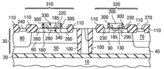
[0009]The instant invention comprises forming a fluorinated IFO in a poly-emitter bipolar junction transistor (BJT). The fluorinated IFO reduces the 1 / f noise in NPN transistors without affecting the HFE or Va of the PNP transistor. The method of fluorinated IFO formation comprises introducing a fluorine containing species into the polysilicon emitter of the NPN BJT during formation. The method will be described with reference to an integrated circuit process for forming PNP and NPN transistors. It should however be noted that the method applies to the formation of a fluorinated IFO and can be used in any semiconductor device requiring an IFO.

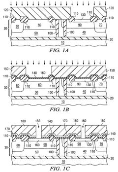
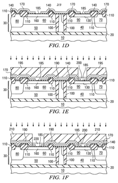
[0010]Shown in FIGS. 1(a)–1(i) are cross-sectional diagrams showing an embodiment of the instant invention. Shown in FIG. 1(a) is a semiconductor substrate after a number of processing steps. As shown in FIG. 1(a), silicon on insulator (SOI) substrates are used in the illustrated embodiment. Silicon on insulator substrates usually comprise a fi...


PUM


Abstract

An interfacial oxide layer (185) is formed in the emitter regions of the NPN transistor (280, 220) and the PNP transistor (290, 200). Fluorine is selectively introduced into the polysilicon emitter region of the NPN transistor (220) to reduce the 1 / f noise in the NPN transistor.

Description

[0001]This application is a divisional of application Ser. No. 10 / 266,476, filed Oct. 8, 2002 now U.S. Pat. No. 6,856,000.FIELD OF THE INVENTION[0002]The present invention relates to a method to reduce the 1 / f noise in NPN transistors without degrading the properties in PNP transistors in integrated circuits containing both NPN and PNP transistors.BACKGROUND OF THE INVENTION[0003]The electrical properties of polycrystalline silicon emitter (poly-emitter) bipolar junction transistors (BJT) are strongly influenced by the properties of the interfacial oxide (IFO) that exists between the polycrystalline silicon (polysilicon) emitter and the crystalline emitter. For example, the current gain (HFE) of the BJT can be enhanced by a thicker IFO layer. The current gain HFE is defined as the ratio of the corresponding change in transistor collector current δIC to a change in the transistor base current δIB. In addition to a higher HFE, an accompanying increase in the Early Voltage (Va) is obta...

Claims


Application Information

Patent Timeline
Patent Type & AuthorityPatents(United States)
IPC IPC(8): H01L21/339H01L21/331H01L21/8228H01L27/082H01L29/08
CPCH01L21/82285H01L29/66287H01L29/0804H01L27/0826
InventorTROGOLO, JOE R.LOFTIN, WILLIAMKYSER, JR., WILLIAM F.
OwnerTEXAS INSTR INC