
Interfacial oxide used as switching layer in a nonvolatile resistive memory element

a nonvolatile resistive memory element and interfacial oxide technology, applied in the direction of bulk negative resistance effect devices, electrical equipment, semiconductor devices, etc., can solve the problems of complex process for forming resistive switching memory devices having suitably small dimensions, scaling issues that pose challenges for traditional nonvolatile memory technology

Inactive Publication Date: 2013-09-05
INTERMOLECULAR
View PDF9 Cites 13 Cited by
  • Summary
  • Abstract
  • Description
  • Claims
  • Application Information

AI Technical Summary

Benefits of technology

This patent describes a new type of nonvolatile memory that uses an interfacial oxide layer formed on the surface of a host oxide layer. This interfacial oxide layer can improve the performance of the memory device and make it more reliable. The method of forming this new memory element involves depositing a layer of host oxide, treating its surface with an oxidation treatment to form an interfacial oxide layer, and then depositing a new layer of electrode material on top of the interfacial oxide layer. This new memory element can be used in a variety of applications and offer improved performance compared to traditional resistive memory elements.

Problems solved by technology

However, as device dimensions shrink, scaling issues pose challenges for traditional nonvolatile memory technology.
In addition, the formation of resistive switching memory devices having suitably small dimensions is a complicated process, requiring a number of different and specialized deposition systems, such as atomic layer deposition and physical vapor deposition systems.

Method used


Image

  • Interfacial oxide used as switching layer in a nonvolatile resistive memory element
  • Interfacial oxide used as switching layer in a nonvolatile resistive memory element
  • Interfacial oxide used as switching layer in a nonvolatile resistive memory element

Examples


Embodiment Construction

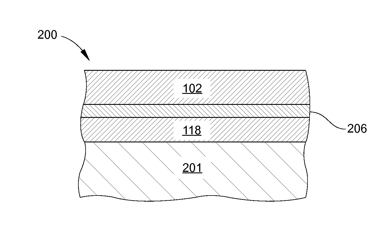
[0020]Materials used as the switching layer of a nonvolatile resistive memory element are generally required to have bistable properties and can be operated with low switching current. Embodiments of the invention set forth a nonvolatile memory element with a novel variable resistance layer and methods of forming the same. The novel variable resistance layer includes a host oxide that is formed from an interfacial oxide and operates with reduced switching voltage and current. The interfacial oxide layer is an oxide layer that may be formed on the surface of a deposited electrode layer via in situ or post-deposition surface oxidation treatments.

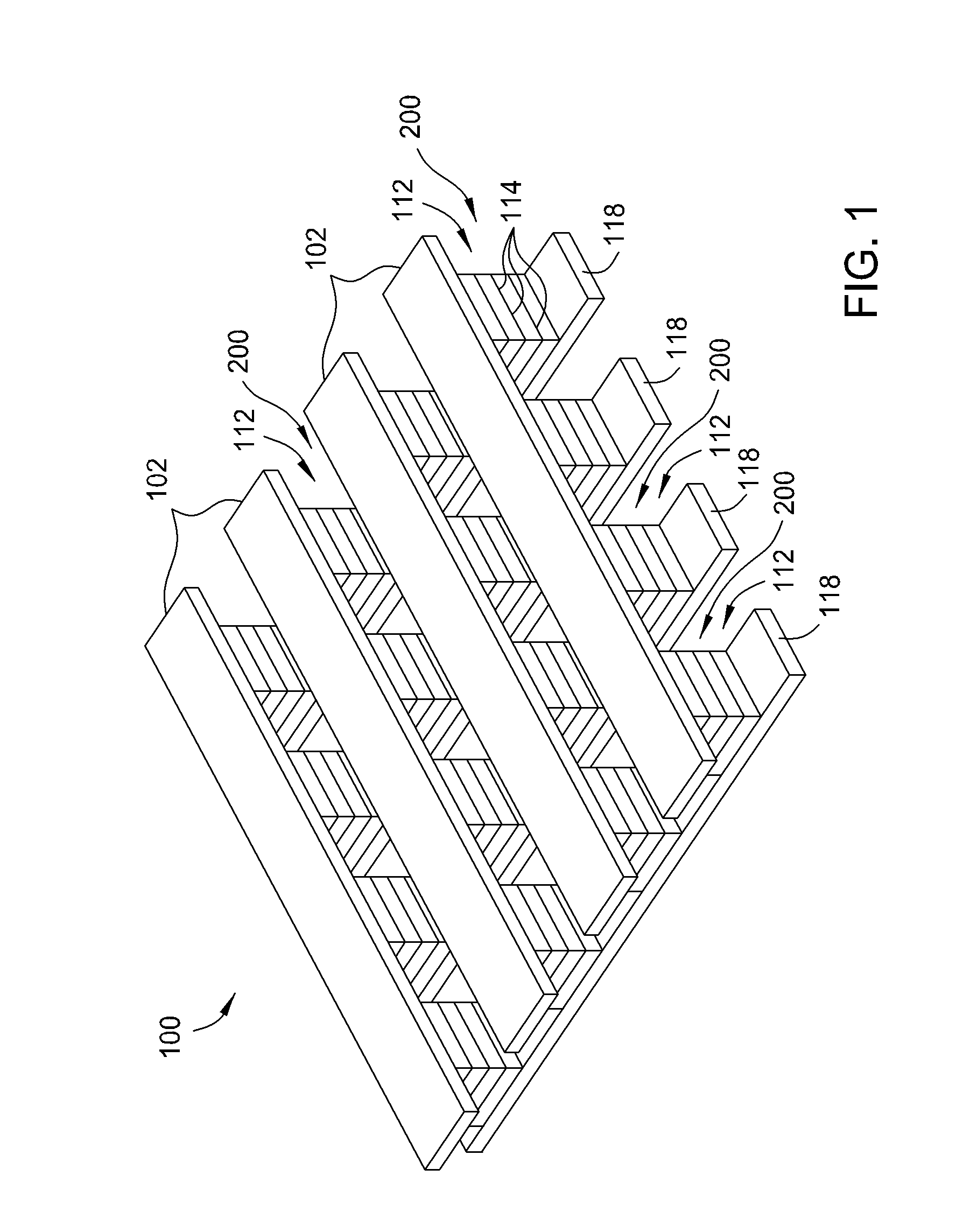
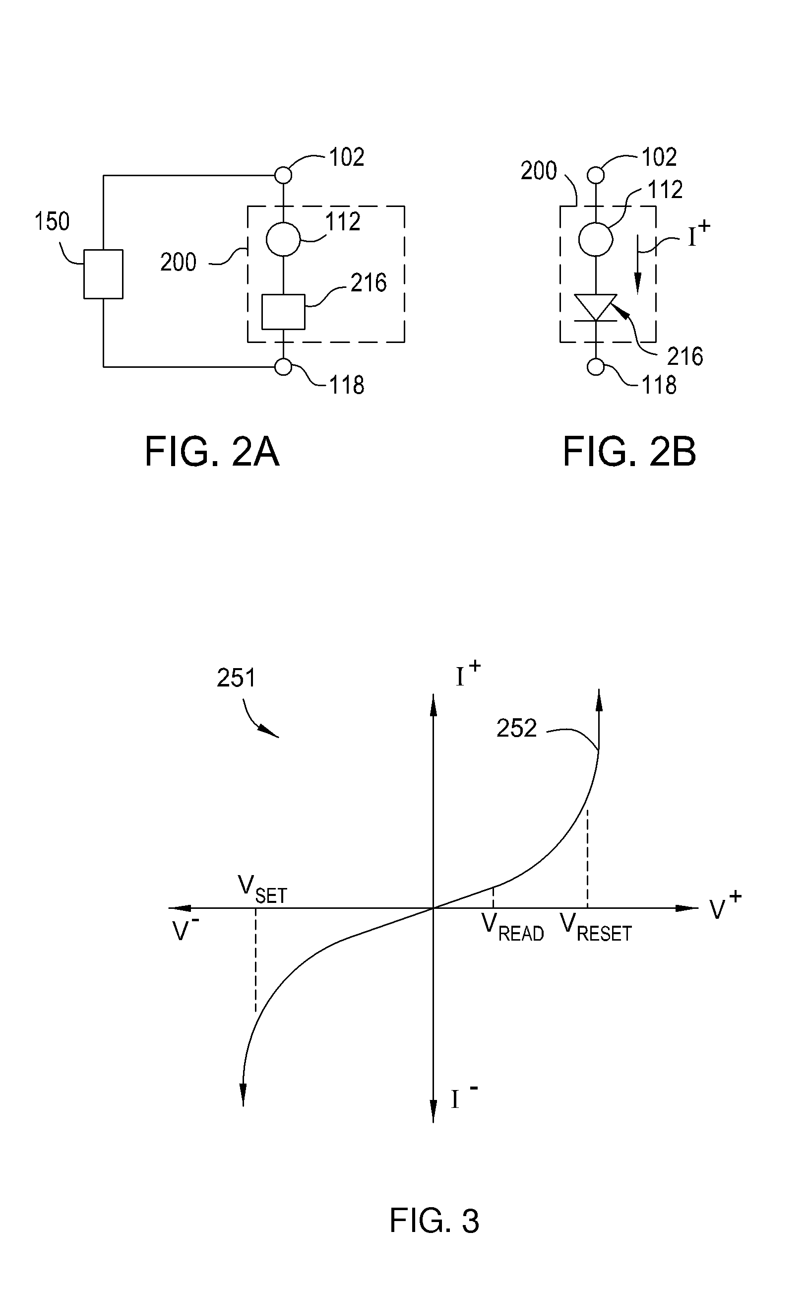
[0021]FIG. 1 is a perspective view of a memory array 100 of memory devices 200, configured according to embodiments of the invention. Memory array 100 may be part of a larger memory device or other integrated circuit structure, such as a system-on-a-chip type device. Memory array 100 may be formed as part of a high-capacity nonvolatile memory ...


PUM


Abstract

A nonvolatile resistive memory element includes a host oxide formed from an interfacial oxide layer. The interfacial oxide layer is formed on the surface of a deposited electrode layer via in situ or post-deposition surface oxidation treatments. The switching performance of a resistive memory device based on such an interfacial oxide layer is equivalent or superior to the performance of a conventional resistive memory element.

Description

BACKGROUND[0001]1. Field of the Invention[0002]This invention relates to nonvolatile resistive memory elements, and more particularly, to the use of an interfacial oxide as a switching layer in a nonvolatile resistive memory element.[0003]2. Description of the Related Art[0004]Nonvolatile memory elements are used in devices requiring persistent data storage, such as digital cameras and digital music players, as well as in computer systems. Electrically-erasable programmable read only memory (EPROM) and NAND flash are nonvolatile memory technologies currently in use. However, as device dimensions shrink, scaling issues pose challenges for traditional nonvolatile memory technology. This has led to the investigation of alternative nonvolatile memory technologies, including resistive switching nonvolatile memory.[0005]Resistive-switching-based nonvolatile memory is formed using memory elements that are bistable, i.e., having two stable states with different resistances. A bistable memor...

Claims


Application Information

Patent Timeline
IPC IPC(8): H01L45/00H01L21/62
CPCH01L45/08H01L45/10H01L45/1233H01L27/2463H01L45/1633H01L45/145H01L27/2409H01L45/146H10B63/20H10B63/80H10N70/25H10N70/24H10N70/883H10N70/028H10N70/8833H10N70/826
Inventor HIGUCHI, RANDALLCHIANG, TONY P.CLARKE, RYANGOPAL, VIDYUTHASHIM, IMRANHUERTAS, ROBERTWANG, YUN
Owner INTERMOLECULAR
Learn More