MOSFETS Having Stacked Metal Gate Electrodes and Method

Inactive Publication Date: 2009-11-12
TAIWAN SEMICON MFG CO LTD
View PDF19 Cites 14 Cited by
  • Summary
  • Abstract
  • Description
  • Claims
  • Application Information

AI Technical Summary

Benefits of technology

[0006]These and other problems are generally solved or circumvented, and technical advantages are generally achieved, by preferred embodiments of the present invention which provide an MOSFET having stacked metal gate electrodes and methods of making the same. The MOSFET gate electrode includes a gate metal layer formed atop a high-k gate dielectr

Problems solved by technology

However, device feature size scaling in advanced technology may lead to a very thin gate SiO2 layer and, thus, the gate leakage current may become unacceptably large.
However, the existing high-k, metal gate MOSFET fabrication approach is problematic in at least the following ways.
Firstly, when a PVD process (e.g., plasma sputtering) is used in metal gate deposition, the ion bombardment involved may cause plasma damage in the high-k gate dielectric and interfacial layer, and thus lead to carrier mobility degradation.

Method used


Image

  • MOSFETS Having Stacked Metal Gate Electrodes and Method
  • MOSFETS Having Stacked Metal Gate Electrodes and Method
  • MOSFETS Having Stacked Metal Gate Electrodes and Method

Examples


Embodiment Construction

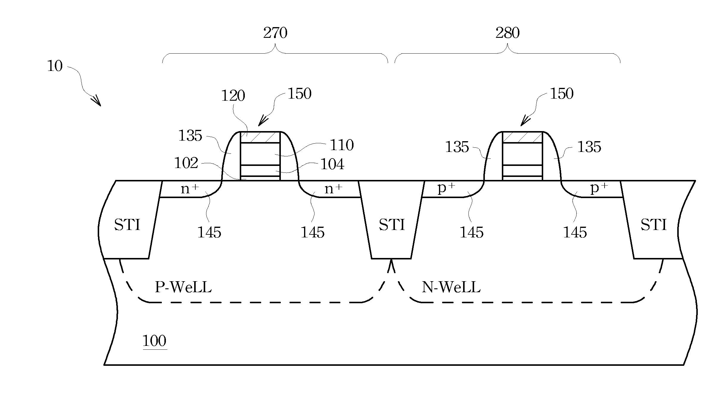
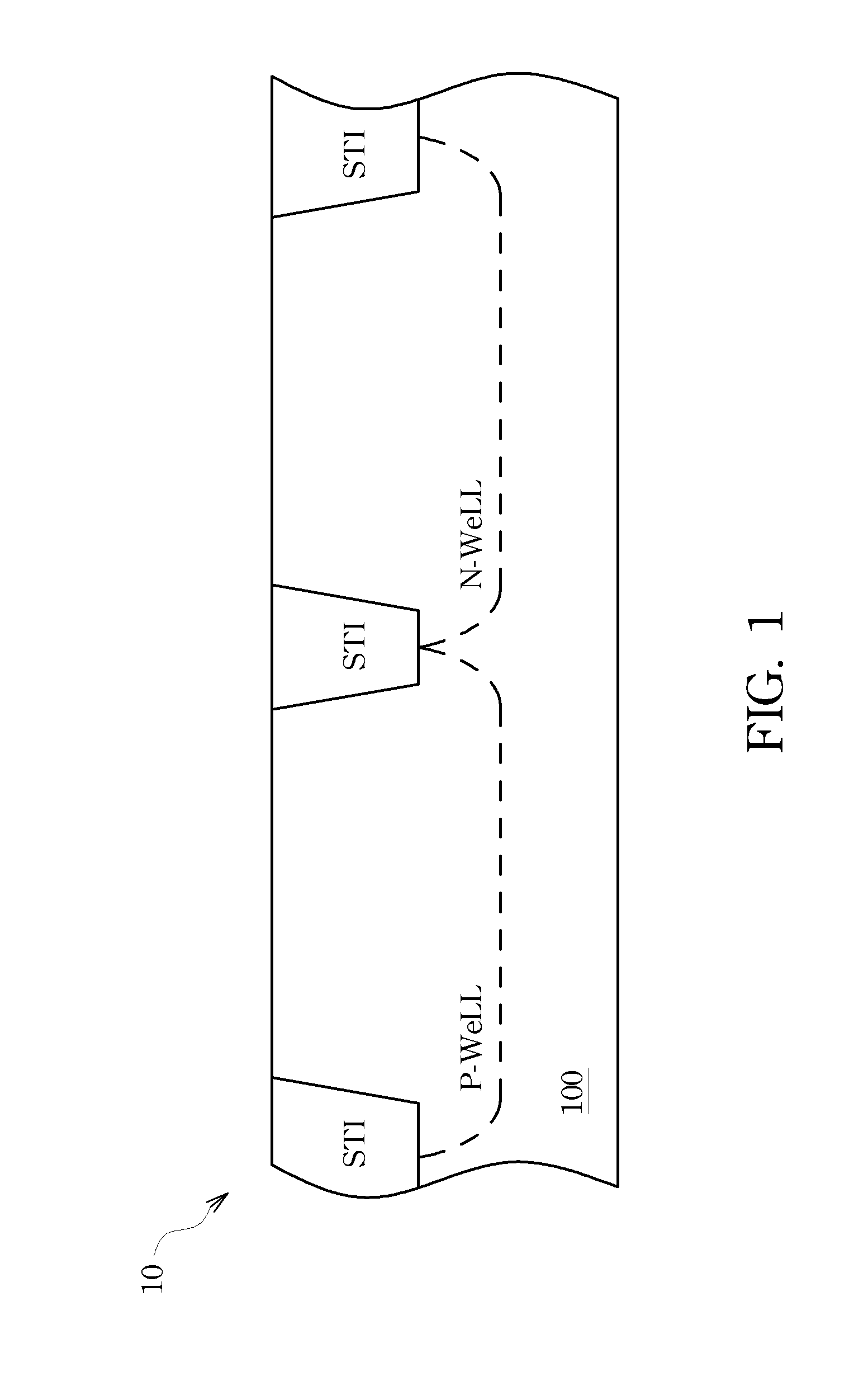
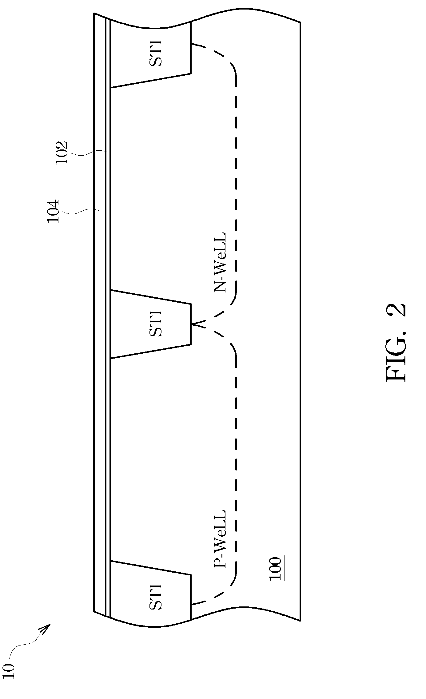
[0015]The making and using of the presently preferred embodiments are discussed in detail below. It should be appreciated, however, that the present invention provides many applicable inventive concepts that can be embodied in a wide variety of specific contexts. The specific embodiments discussed are merely illustrative of specific ways to make and use the invention, and do not limit the scope of the invention.

[0016]The present invention will be described with respect to preferred embodiments in a specific context, namely MOSFETs having a high-k gate dielectric layer and a stacked metal gate electrode with reduced or minimized plasma damage and interfacial layer regrowth, and a method of forming the same. Embodiments of the present invention may also be applied, however, to other transistor structures and methods of fabrication thereof. Cross-sectional views of processing steps are shown for fabricating MOSFETs in preferred embodiments using a CMOS manufacturing process flow. While...


PUM


Abstract

MOSFETs having stacked metal gate electrodes and methods of making the same are provided. The MOSFET gate electrode includes a gate metal layer formed atop a high-k gate dielectric layer. The metal gate electrode is formed through a low oxygen content deposition process without charged-ion bombardment to the wafer substrate. Metal gate layer thus formed has low oxygen content and may prevent interfacial oxide layer regrowth. The process of forming the gate metal layer generally avoids plasma damage to the wafer substrate.

Description

TECHNICAL FIELD[0001]The present invention relates generally to structures of metal oxide semiconductor field effect transistors (MOSFETs) in integrated circuits and methods of making the same, and more particularly to MOSFETs having stacked metal gate electrodes, and methods of fabricating the same.BACKGROUND[0002]While the scaling down of the device feature size in a semiconductor integrated circuit (IC) continues in the pursuit of smaller, faster, and more complex circuit functions on a single integrated circuit, maintaining high drive current at scaled voltages and smaller MOSFET gate dimensions generally becomes more important. Device drive current is closely related to parameters such as gate dimension, gate capacitance, and carrier mobility. Among the various technology innovations made to maintain high MOSFET drive current, high-k (dielectric constant) gate dielectrics and metal gate electrodes are commonly adopted to increase gate capacitance of MOSFETs in advanced technolo...

Claims


Application Information

Patent Timeline
IPC IPC(8): H01L21/3205
CPCH01L21/28079H01L21/28088H01L21/28185H01L29/517H01L21/823437H01L21/823828H01L29/513H01L21/3141H01L21/0228
Inventor LIN, CHENG-TUNGCHIU, YUNG-SHENGWANG, HSIANG-YIYU, CHIA-LINYU, CHEN-HUA
Owner TAIWAN SEMICON MFG CO LTD
Why Eureka
Try Eureka