Semiconductor device and method of fabricating the same

a technology of semiconductors and semiconductors, applied in semiconductor devices, electrical devices, transistors, etc., can solve the problems of crystal grain boundary distortion and micro crack formation, and achieve the effect of reducing the density of bulk defects and the density of interface defects

Inactive Publication Date: 2006-03-21
SEMICON ENERGY LAB CO LTD
View PDF32 Cites 35 Cited by
  • Summary
  • Abstract
  • Description
  • Claims
  • Application Information

AI Technical Summary

Benefits of technology

[0016]An object of the present invention is to solve the foregoing problem and to realize a TFT in which bulk defect density and interface defect density are decreased while distortion is not generated in a crystalline semiconductor layer.

Problems solved by technology

In all events, when the crystalline semiconductor film is contracted, if a stress acts in a direction to expand this, it is expected that distortion occurs in crystal grain boundaries and micro cracks are formed.

Method used


Image

  • Semiconductor device and method of fabricating the same
  • Semiconductor device and method of fabricating the same
  • Semiconductor device and method of fabricating the same

Examples


embodiment mode 1

[Embodiment Mode 1]

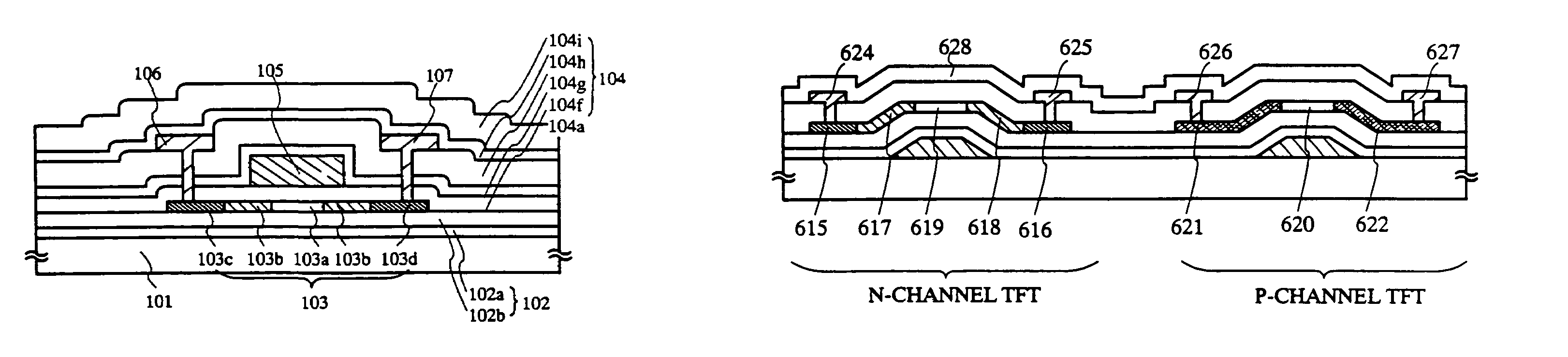
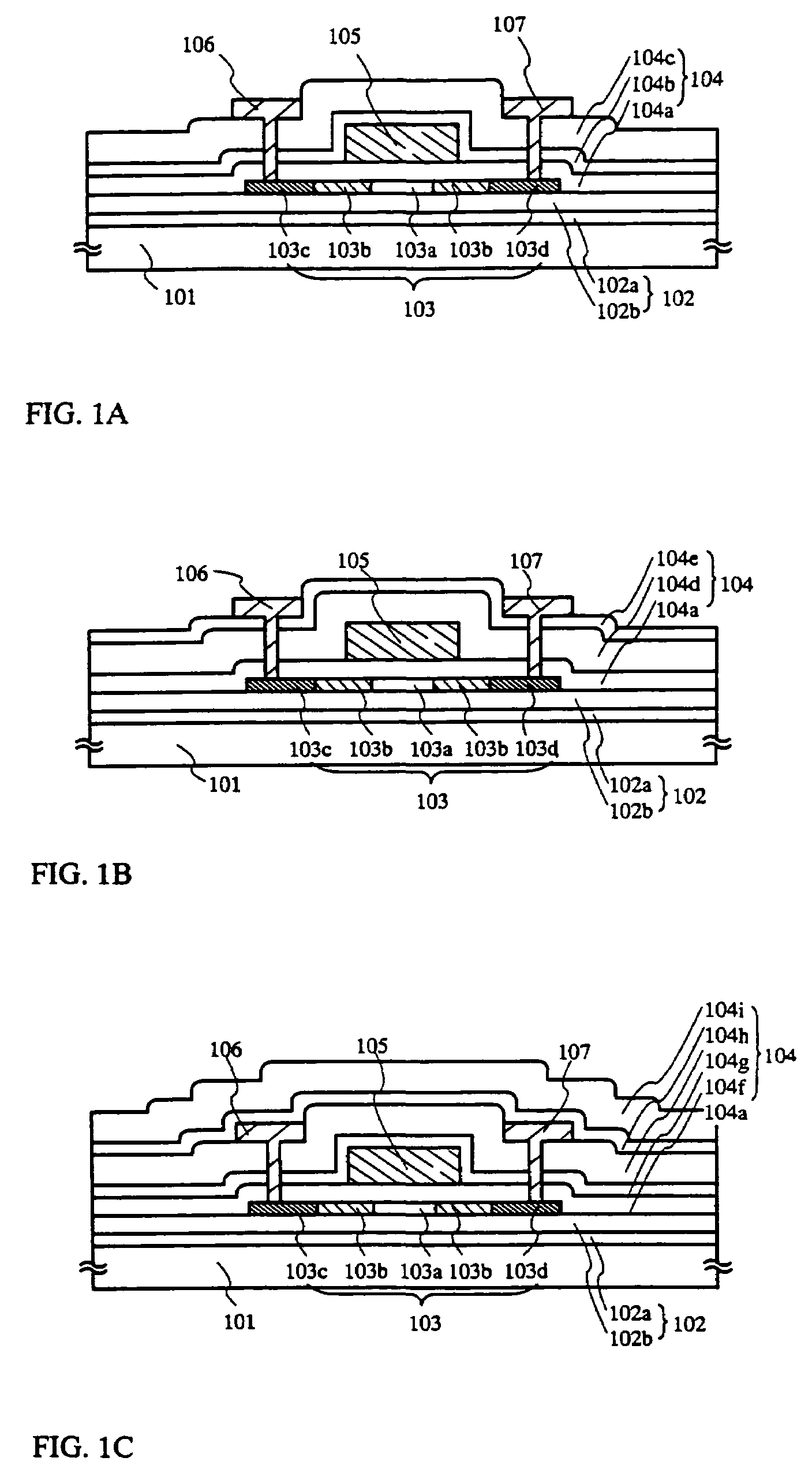
[0066]A first embodiment mode for carrying out the invention will be described with reference to FIGS. 1A to 1C. In FIGS. 1A to 1C, a first insulating layer 102 is formed on a substrate 101 having an insulating surface. The first insulating layer 102 is formed of a nitrogen-rich silicon nitride oxide film 102a having a nitrogen content of not less than 25 atomic % and less than 50 atomic % and a silicon nitride oxide film 102b having a nitrogen content of not less than 5 atomic % and less than 25 atomic % in this order from the substrate. The nitrogen-rich silicon nitride oxide film 102a has a tensile stress of 5×10⁸ Pa to 2×10⁹ Pa. The silicon nitride oxide film 102b is a film having a compressive stress of not higher than −5×10⁸ Pa, and is provided between the nitrogen-rich silicon nitride oxide film 102a and an active layer 103 so as to slightly relieve the action of stress.

[0067]The active layer 103 is a crystalline semiconductor film fabricated from an amorph...

embodiment mode 2

[Embodiment Mode 2]

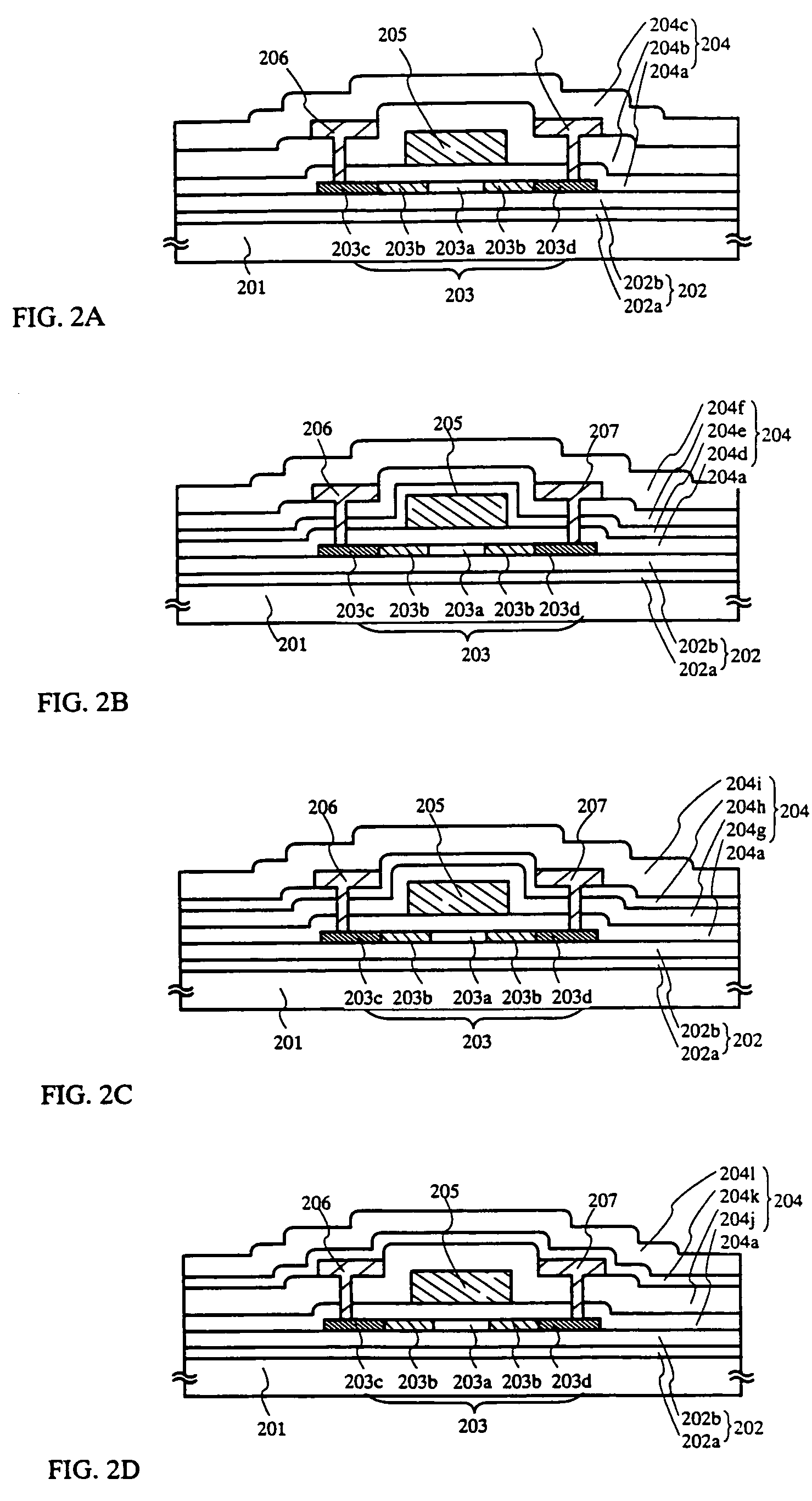
[0072]A second embodiment mode for carrying out the invention will be described with reference to FIGS. 2A to 2D. In FIGS. 2A to 2D, a first insulating layer 202 is formed on a substrate 201 having an insulating surface. Similarly to Embodiment Mode 1, a nitrogen-rich silicon nitride oxide film 202a having a nitrogen content of not less than 25 atomic % and less than 50 atomic %, and a silicon nitride oxide film 202b having a nitrogen content of not less than 5 atomic % and less than 25 atomic % are provided. The nitrogen-rich silicon nitride oxide film 202a has tensile stress. An active layer 203 is a crystalline semiconductor film fabricated from an amorphous semiconductor film by a method such as a laser annealing method or a thermal annealing method, and as the need arises, a channel formation region 203a, LDD regions 203b, a source region 203c, and a drain region 203d are provided. Contact holes are provided in part of a second insulating layer 204 so that a ...

embodiment 1

[Embodiment 1]

[0077]This embodiment will be described with reference to FIGS. 5A to 7D as an example of a bottom gate type TFT. First, a glass substrate, for example, a #1737 substrate of Corning Inc. was prepared as a substrate 601. A gate electrode 602 was formed on the substrate 601. Here, a tantalum (Ta) film was formed to a thickness of 200 nm by using a sputtering method. The gate electrode 602 may be a two-layer structure of a tantalum nitride film (film thickness of 50 nm) and a Ta film (film thickness of 250 nm). The Ta film was formed by a sputtering method using an Ar gas while Ta was used as a target, and when sputtering was made with a mixture gas of the Ar gas added with a Xe gas, it was possible to make an absolute value of an internal stress 2×10⁸ Pa or less (FIG. 5A).

[0078]Then, a first insulating layer 603 and an amorphous semiconductor layer 604 were continuously formed without opening to the air. The first insulating layer 603 was formed of a nitrogen-rich silico...


PUM


Abstract

In a semiconductor device including a laminate of a first insulating layer, a crystalline semiconductor layer, and a second insulating layer, characteristics of the device are improved by determining its structure in view of stress balance. In the semiconductor device including an active layer of the crystalline semiconductor layer having tensile stress on a substrate, tensile stress is given to the first insulating layer formed to be in close contact with a surface of the semiconductor layer at a substrate side, and compressive stress is given to the second insulating layer formed to be in close contact with a surface of the semiconductor layer at a side opposite to the substrate side.

Description

[0001]This application is a divisional of U.S. application Ser. No. 10 / 093,313, filed on Mar. 7, 2002 now U.S. Pat. No. 6,645,826 which is a divisional of U.S. application Ser. No. 09 / 472,137, filed on Dec. 23, 1999 (now U.S. Pat. No. 6,380,558).BACKGROUND OF THE INVENTION[0002]1. Field of the Invention[0003]The present invention relates to a semiconductor device including an integrated circuit using thin film transistors on a substrate and a method of fabricating the same. Particularly the invention relates to a structure of, for example, an electro-optical device typified by a liquid crystal display device and an electronic equipment incorporating the electro-optical device.[0004]2. Description of the Related Art[0005]Development has been made on a semiconductor device typified by an active matrix type liquid crystal display device in which a number of TFTs (thin film transistors) are arranged on a substrate. The TFT has a laminate structure including at least an active layer made...

Claims


Application Information

Patent Timeline
Patent Type & Authority Patents(United States)
IPC IPC(8): H01L29/04H01L31/036H01L31/0376H01L31/20H01L21/336H01L21/77H01L21/84H01L27/12H01L29/786
CPCH01L27/12H01L29/66757H01L29/66765H01L29/7842H01L29/78603H01L27/1277H01L29/78627H01L29/78636H01L29/78645H01L27/1248H01L29/78621H01L2029/7863
Inventor YAMAZAKI, SHUNPEIASAMI, TAKETOMITAKAYAMA, TORUKAWASAKI, RITSUKOADACHI, HIROKISAKAMOTO, NAOYAHAYAKAWA, MASAHIKOSHIBATA, HIROSHIARAI, YASUYUKI
Owner SEMICON ENERGY LAB CO LTD
Why Eureka
Try Eureka