

Method for manufacturing of a mask blank for EUV photolithography and mask blank
- Summary
- Abstract
- Description
- Claims
- Application Information
AI Technical Summary
Benefits of technology
Problems solved by technology
Method used
Image

Examples
example 1
MEASUREMENT RESULTS OF EXAMPLE 1
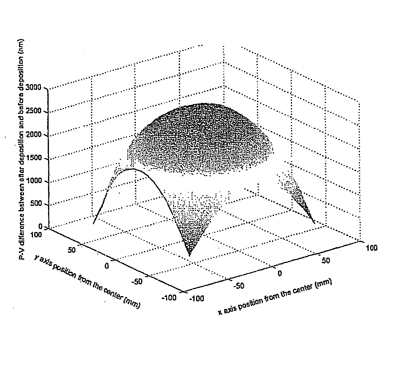
[0072]FIG. 4b shows a three-dimensional plot of stress induced in a tantalum nitride (TaN) film according to example 1, as measured by a peak-to-valley bending of said substrate after depositing said film, for ion beam sputtering (IBS) using Xenon (Xe) ions. The peak-to-valley bending is approx. 1.56 micron for a 6×6 Inch square photo mask blank. As is know to a person skilled in the art the value for the bending of the photo mask blank can be converted into stress values in units of MPa.
[0073] The tantalum nitride absorber layer showed a high etch selectivity with an etch bias of almost 0 with 100% over etch. Features smaller than 100 nm could be achieved, the CD uniformity was less than 10 nm.
[0074]FIG. 3 shows results of reflection measurements at two different optical inspection wavelengths in the near ultraviolet spectral range in a two-dimensional plot of the photo mask blank according to example 1. At an optical inspection wavelength of 365 n...
reference example 2
[0080] In a reference example, Argon (Ar) is used as the sputter gas, with 1500 kV energy of the first ion beam and a current of 200 mA. The bottom tantalum layer with a thickness of 50 nm was doped with nitrogen in the presence of a nitrogen flow of 30 sccm. On top of the tantalum layer a 20 nm thick TaON layer was deposited. This layer was doped with nitrogen using a nitrogen flow of 30 sccm and with oxygen using an oxygen flow of 15 sccm. Hence, besides using Ar ions instead of Xe ions, identical parameters were used for ion beam sputtering the TaN and TaON layers.
example 2
MEASUREMENT RESULTS OF EXAMPLE 2
[0081]FIG. 4a shows a three-dimensional plot of stress induced in a tantalum nitride (TaN) film according to example 2, as measured by a peak-to-valley bending of said substrate after depositing said film, for ion beam sputtering (IBS) using Argon (Ar) ions. The peak-to-valley bending is approx. 2.62 micron for a 6×6 Inch square photo mask blank. Hence, for similar process parameters the stress induced in the tantalum nitride absorber layer is substantially higher when Argon ions are used as sputter gas for ion beam sputtering.
[0082] Further aspects according to the present invention concerning the conductive coating provided on the back surface of the substrate are disclosed in the applicant's co-pending U.S. patent application Ser. No. 10 / 825,618 filed on Apr. 16, 2004 ‘Mask blank for use in EUV lithography and method for its production’ and in the applicant's German patent application no. 103 17 792.2-51 filed on Apr. 16, 2003, the whole contents ...
PUM
| Property | Measurement | Unit |
|---|---|---|
| Length | aaaaa | aaaaa |
| Length | aaaaa | aaaaa |
| Fraction | aaaaa | aaaaa |
Abstract
Description
Claims
Application Information