Production method of strained silicon-SOI substrate and strained silicon-SOI substrate produced by same

a production method and technology of silicon-soi substrate, which are applied in the direction of basic electric elements, electrical apparatus, semiconductor devices, etc., can solve the problems of insufficient surface roughness, insufficient penetrating dislocation densities and surface roughness of the sige layer, and difficult to retain such a compatible effect within a micro device having a gate length not more than 100 nm, etc., to achieve enhanced strain relaxation of the sige mixed crystal layer, low defect density, and weaken bond strength

Inactive Publication Date: 2006-09-28
SUMCO CORP +1
View PDF14 Cites 46 Cited by
  • Summary
  • Abstract
  • Description
  • Claims
  • Application Information

AI Technical Summary

Benefits of technology

[0050] In the present invention, a production method of a strained Si-SOI substrate comprises: growing an SiGe mixed layer on an SOI substrate having an Si layer of not less than 5 nm and less than 100 nm in thickness, and a buried oxide layer; forming a protective film on the SiGe mixed layer; implanting ions into a vicinity of the Si layer and the buried oxide layer; a first heat treatment for heat treating the substrate at a temperature of 400 to 1000° C. in an inert gas atmosphere; a second heat treatment for heat treating the substrate at a temperature not less than 1050° C. in an oxidizing atmosphere containing chlorine; and forming a strained Si layer. By the heat treatment in an oxidizing atmosphere containing chlorine, Ge is caused to diffuse into the Si layer from the SiGe mixed crystal layer and therby change the Si layer into a SiGe mixed layer. At the same time, the light element implanted weakens the bonding strength between the single crystalline silicon layer and the buried oxide layer, and thereby enhances strain relaxation of the SiGe mixed crystal layer. Accordingly, it is possible to obtain a relaxed SiGe layer and a strained Si layer having a low defect density and a flat surface.

Problems solved by technology

However, it is difficult to retain such a compatible effects within a micro device having a gate length of not more than 100 nm.
For example, in the case of using a buffer layer in which Ge content increases with moderate gradient, generation of dislocations causes surface irregularities on the SiGe surface.
Since the surface irregularities have an adverse effect on the photo-lithography which is carried out during a device-production process, it is needed to remove the irregularities.
However, even after the polishing step, penetrating dislocation densities and surface roughness of the SiGe layer have been in an insufficient state compared with the desirable level for a device or a desirable level for raw materials for device production.
Especially, the above described cross-hatches are not uniformly distributed.
It has been difficult to polish off such surface irregularities of cross-hatches during polishing of the SiGe using a general method for polishing the Si.
Therefore, such a method has involved high production cost.
The above described method raises the problem of relatively long operation time for melting the amorphous SiGe layer and amorphous Si layer, and removal of the oxide layer.

Method used


Image

  • Production method of strained silicon-SOI substrate and strained silicon-SOI substrate produced by same
  • Production method of strained silicon-SOI substrate and strained silicon-SOI substrate produced by same
  • Production method of strained silicon-SOI substrate and strained silicon-SOI substrate produced by same

Examples


first embodiment

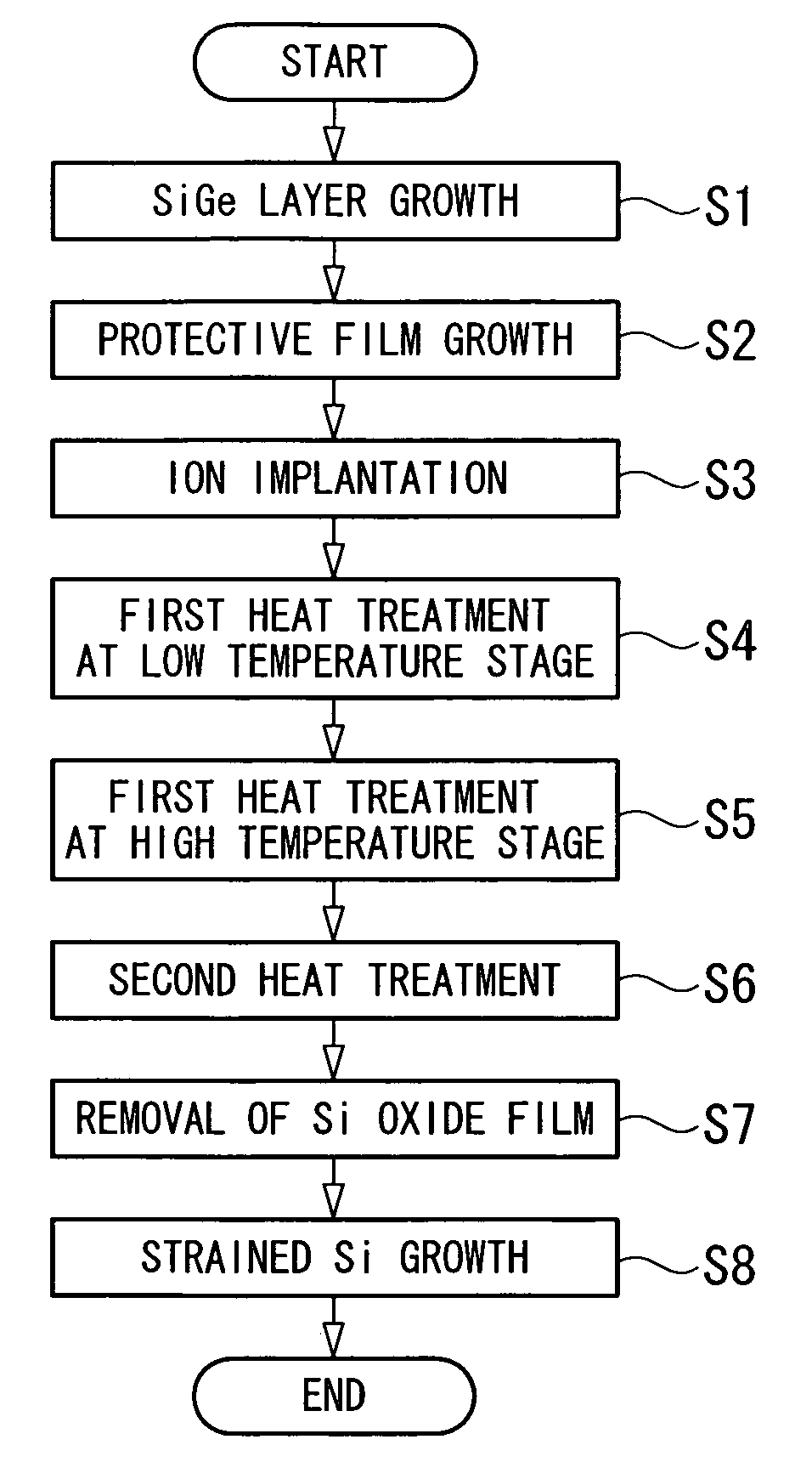
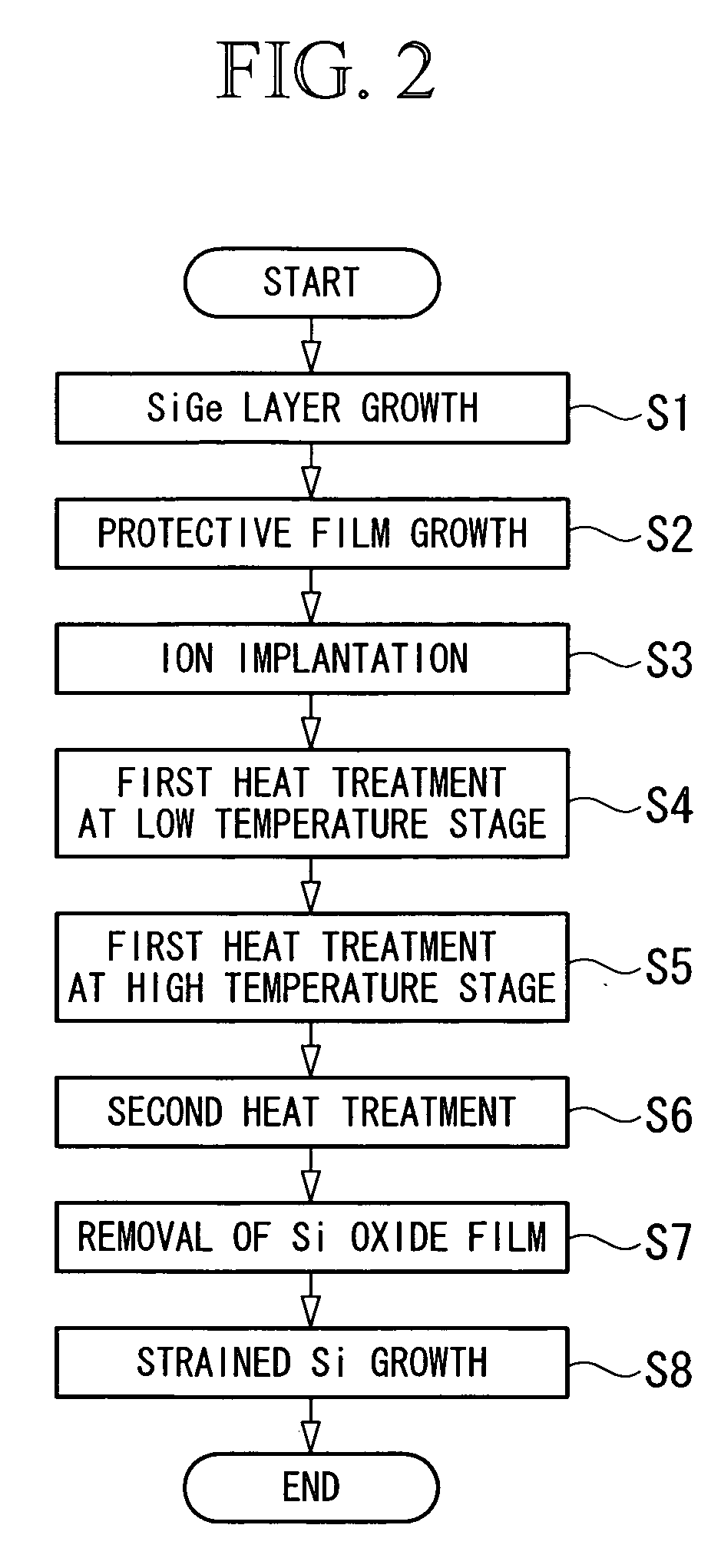
[0059] A first embodiment of a production method of a strained Si-SOI substrate of the invention is explained with reference to the drawings.

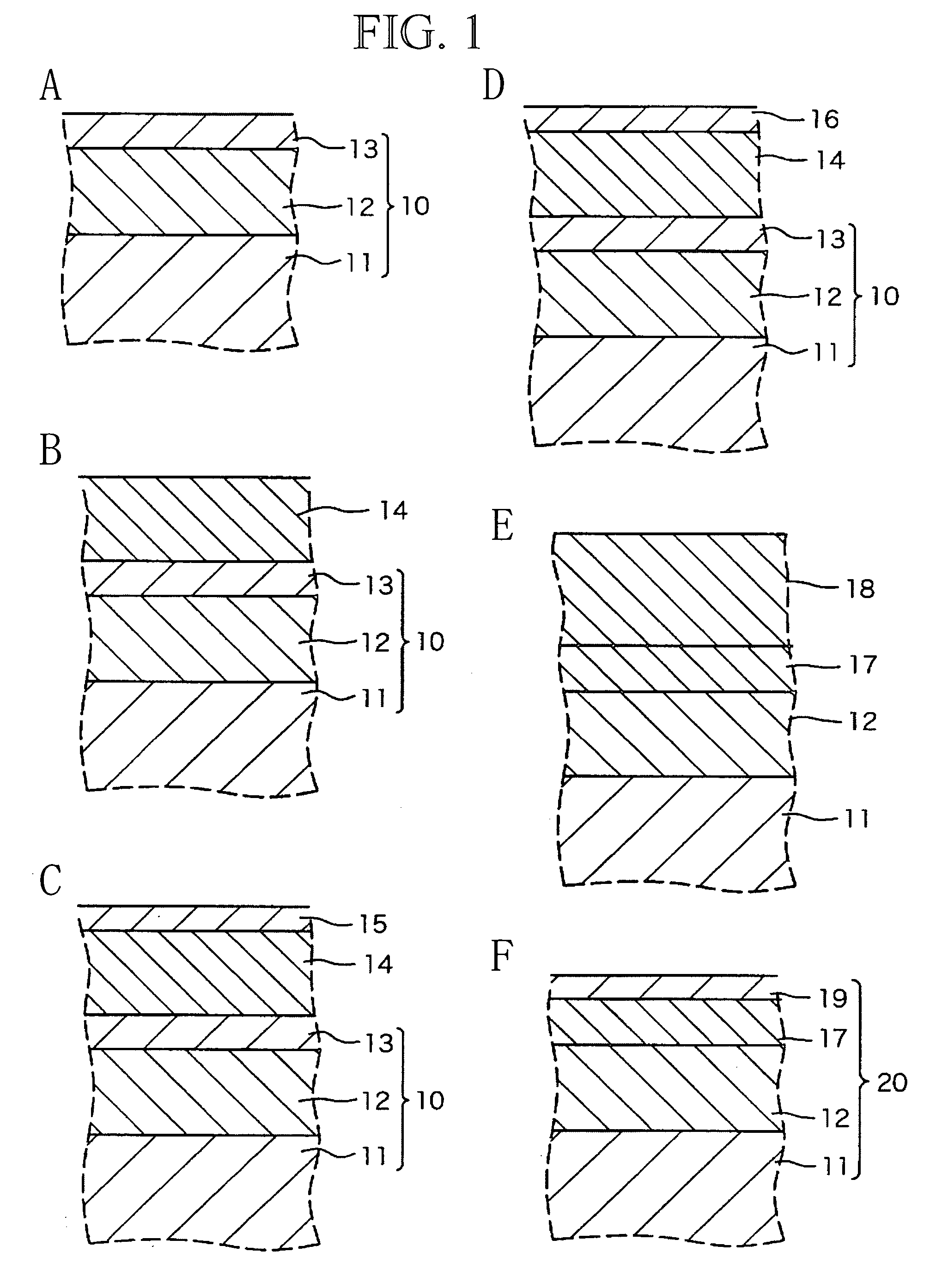
[0060]FIGS. 1A to 1F are cross sectional views of substrates showing a production process of a strained Si-SOI substrate. FIG. 2 is a process chart showing a production method of a strained Si-SOI substrate in the embodiment. In FIG. 1 the SOI substrate is indicated by numeral 10.

[0061] A strained Si-SOI substrate is produced by the following method.

[0062] Firstly, an SOI substrate 10 is prepared. The SOI substrate 10 comprises an insulator layer (buried oxide layer) 12 on an Si substrate 11, and a single crystalline Si layer (Si layer) 13 on the insulator layer 12. For example, as the SOI substrate 10, it is possible to use an SOI substrate produced by the SIMOX (Separation by IMplanted OXgen) method. In the SIMOX method, by oxygen implantation from a surface of a wafer, a buried oxide layer (a BOX layer) is formed in a portion having a pre...

second embodiment

[0086] Next, a second embodiment of a production method of a strained Si-SOI substrate is explained with reference to the drawings. FIG. 5 is a process chart showing the production method of a strained Si-SOI substrate in accordance with the second embodiment. An explanation for the elements corresponding to the elements of the first embodiment is omitted because the same symbols are used.

[0087] An SOI wafer 10 is prepared to comprise an Si layer 13 of not less than 5 nm in thickness in a buried oxide layer 12.

[0088] The SOI substrate may be produced by a known method such as the SIMOX method, or a bonding method (e.g., Smart-Cutting method, or ELTRAN method).

[0089] As a next step shown in S11 of FIG. 5, the SOI substrate 10 for forming a SiGe layer 14 is subjected to cleaning. The method for cleaning the SOI substrate may be selected from conventional cleaning methods such as SC-1+SC-2 cleaning, cleaning with a mixing solution of HF / O3, and reciprocal cleaning alternately using ...

example 1

1) Example 1

[0108] P-type SOI substrates of 200 mm in diameter were prepared by the SIMOX method. In each wafer, a thickness of a single crystalline Si layer 13 on a buried oxide layer 12 was 50 nm, and a thickness of the buried oxide layer 12 was 140 nm.

[0109] Subsequently, after cleaning of each SOI wafer (SOI substrate) 10 by the SC-1+SC-2 cleaning method, the wafer was immediately introduced to the lamp heater type single wafer type epitaxial growth apparatus.

[0110] Before the epitaxial growth of the SiGe layer, the SOI wafer was subjected to a hydrogen baking treatment. For the baking, the temperature was at 1125° C., atmospheric pressure was 2666 Pa (20 torr), a hydrogen flow rate was 20 SLM (liter per minutes at standard state), and the time was 45 seconds.

[0111] After cleaning of the surface of the substrate 10 by hydrogen baking treatment, a SiGe layer 14 was epitaxially grown. The thickness of the SiGe layer was 100 nm, and its Ge concentration was 10 atomic %.

[0112] F...


PUM

PropertyMeasurementUnit
thicknessaaaaaaaaaa
temperatureaaaaaaaaaa

Abstract

A strained Si-SOI substrate is produced by a method comprising: growing a SiGe mixed crystal layer on an SOI substrate having a Si layer of not less than 5 nm in thickness and a buried oxide layer; forming a protective film on the SiGe mixed crystal layer; implanting light element ions into a vicinity of an interface between the silicon layer and the buried oxide layer; a first heat treatment for heat treating the substrate at a temperature of 400 to 1000° C. in an inert gas atmosphere; a second heat treatment for heat treating the substrate at a temperature not lower than 1050° C. in an oxidizing atmosphere containing chlorine; removing an oxide film from the surface of the substrate, and forming a strained silicon layer on the surface of the substrate.

Description

BACKGROUND OF THE INVENTION [0001] 1. Field of the Invention [0002] The present invention relates to a strained Si-SOI (Silicon-On-Insulator) substrate of high quality and a method for producing the same. Specifically, the present invention relates to a technology for reducing surface roughness, decreasing number of defects, and improving quality of SOI wafers having a relaxed SiGe layer and a strained Si layer on an oxide film layer. Priority is claimed on Japanese Patent Application No. 2005-090084, filed Mar. 25, 2005, the content of which is incorporated herein by reference. [0003] 2. Description of Related Art [0004] High speed current and low power consumption in silicon MOS devices have been realized compatibly depending on the Scaling law, for example, by minimizing device size, or by decreasing operation voltage. However, it is difficult to retain such a compatible effects within a micro device having a gate length of not more than 100 nm. [0005] Accordingly, introduction o...

Claims


Application Information

Patent Timeline
Patent Type & Authority Applications(United States)
IPC IPC(8): H01L21/00H01L29/00
CPCH01L21/02381H01L21/02532H01L21/26506H01L21/324H01L21/76251H01L21/20H01L27/12
Inventor NINOMIYA, MASAHARUMATSUMOTO, KOJINAKAMAE, MASAHIKOMIYAO, MASANOBU
Owner SUMCO CORP
Why Eureka
Try Eureka