Bonding method

a bonding method and bonding technology, applied in heat-activated film/foil adhesives, solid-state devices, semiconductor devices, etc., can solve the problems of low bonding strength of silicon substrates and piezoelectric substrates, cracks tend to occur, etc., and achieve the effect of improving bonding strength

Active Publication Date: 2019-01-31
NGK INSULATORS LTD
View PDF0 Cites 23 Cited by
  • Summary
  • Abstract
  • Description
  • Claims
  • Application Information

AI Technical Summary

Benefits of technology

[0028]According to the present invention, when a piezoelectric material substrate and a supporting body composed of a singl

Problems solved by technology

However, as the bonding temperature is made high, cracks tend to occur due to a difference of the silicon substrate and piezoelectric substrate.
However, according to this meth

Method used


Image

  • Bonding method
  • Bonding method
  • Bonding method

Examples


example a1

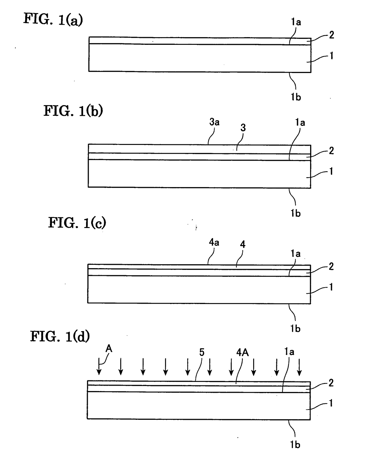
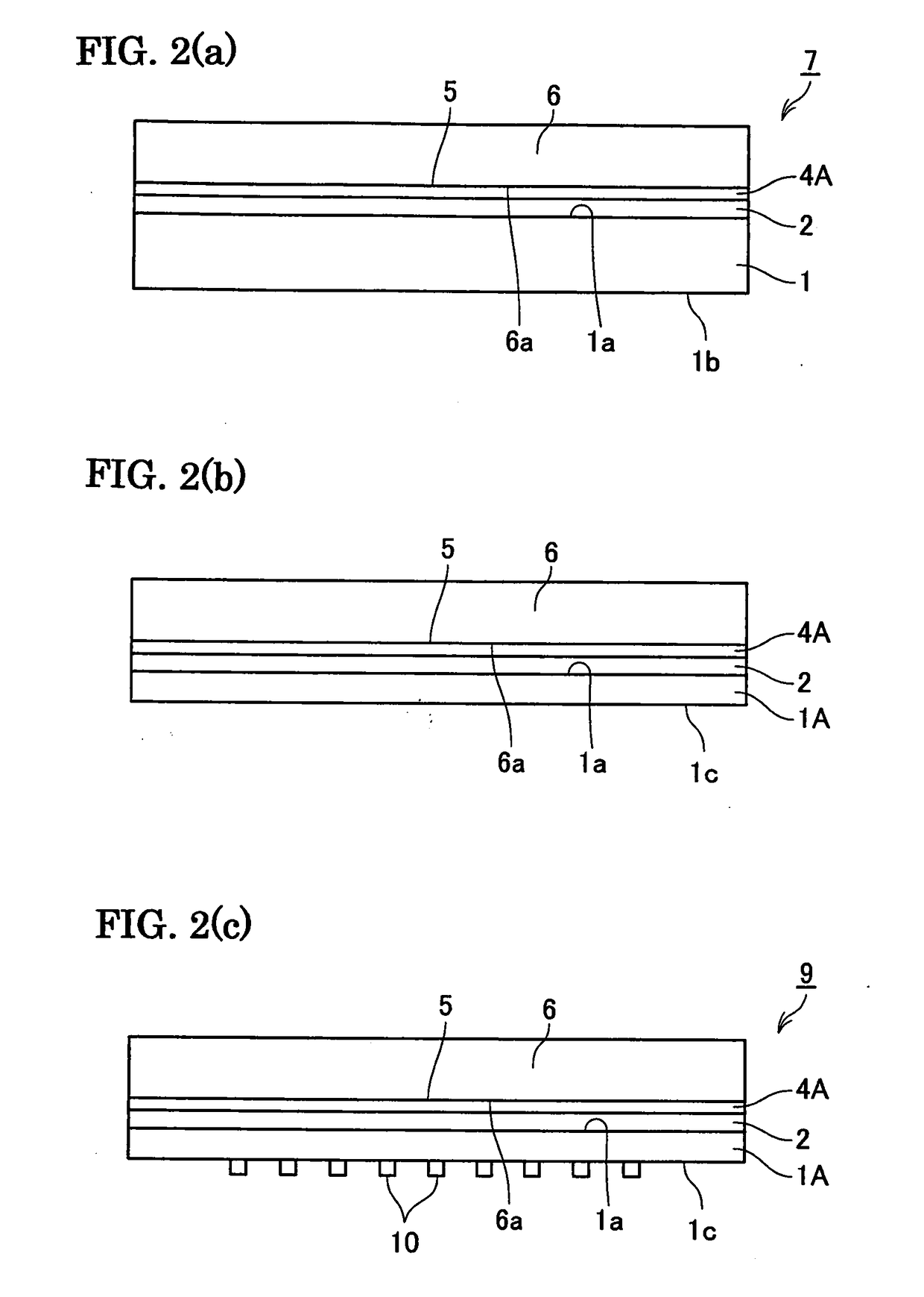
[0098]A bonded body was produced, according to the method of the first invention, described referring to FIGS. 1 and 2.

[0099]Specifically, a substrate (LT substrate) of lithium tantalate having an orientation flat (OF) part, a diameter of 4 inches and thickness of 250 μm was used as the piezoelectric material substrate 1. Further, as the supporting body 6, it was prepared a body having an OF part, a diameter of 4 inches, a thickness of 230 μm and made of silicon. As the LT substrate, it was used LT substrate of 46° Y-cut X-propagation LT substrate, in which the direction of propagation of the surface acoustic wave (SAW) is X and the Y-cut plate is rotated in a cutting angle. The surface 1a of the piezoelectric material substrate 1 and the surface 6a of the supporting body 6 were mirror-polished to an arithmetic average roughness Ra of 1 nm. The arithmetic average roughness was measured by an atomic force microscope (AFM) in a visual field of a square of length of 10 μm and a width o...

example a2

[0103]In the Example A1, the material of the bonding layer 3 was made alumina and the film-formation of the bonding layer 3 was performed by sputtering method. The other procedures were same as those in the Example A1 to produce the bonded body.

[0104]As a result, the separation of the bonded parts was not observed during the grinding and polishing steps of the piezoelectric material substrate. Further, the bonding strength was evaluated by crack opening method and proved to be 1.4 J / m2.

example a3

[0105]In the Example A1, the material of the bonding layer 3 was made tantalum pentoxide (Ta2O5) and the film-formation of the bonding layer was performed by sputtering method. The other procedures were same as those in the Example A1 to produce the bonded body.

[0106]As a result, the separation of the bonded parts was not observed during the grinding and polishing steps of the piezoelectric material substrate. Further, the bonding strength was evaluated by crack opening method and proved to be 1.5 J / m2.


PUM

PropertyMeasurementUnit
Piezoelectricityaaaaaaaaaa

Abstract

A bonding layer 3 is formed over a piezoelectric material substrate, and the bonding layer 3 is made of or more material selected from the group consisting of silicon nitride, aluminum nitride, alumina, tantalum pentoxide, mullite, niobium pentoxide and titanium oxide. Neutralized beam A is irradiated onto a surface 4 of the bonding layer and a surface of a supporting body to activate the surface of the bonding layer and the surface of the supporting body. The surface of the bonding layer and the surface of the supporting body are bonded by direct bonding.

Description

CROSS-REFERENCE TO RELATED APPLICATIONS[0001]This is a continuation of International Application No. PCT / JP2017 / 006461, filed Feb. 22, 2017, which claims priority of Japanese Patent Application No. 2016-061710, filed Mar. 25, 2016, the entire contents of which are incorporated herein by reference.TECHNICAL FIELD[0002]The present invention relates to a method of bonding a piezoelectric material substrate and a supporting body composed of a single crystal.BACKGROUND ARTS[0003]It is known a surface acoustic wave device functioning as a filter device or oscillator used in mobile phones or the like and an acoustic wave device such as lamb wave device or film bulk acoustic resonator (FBAR) using a piezoelectric thin film. As such acoustic wave device, it is known a device produced by adhering a supporting body and a piezoelectric substrate propagating a surface acoustic wave and by providing interdigitated electrodes capable of oscillating the surface acoustic wave on a surface of the pie...

Claims


Application Information

Patent Timeline
IPC IPC(8): H01L41/313H03H9/145H03H9/02H03H9/25H03H3/08H03H9/05H03H9/17H01L41/187H01L41/337H01L41/39
CPCH01L41/313H03H9/145H03H9/02559H03H9/25H03H3/08H03H9/0585H03H9/17H01L41/1871H01L41/1873H01L41/337H01L41/39H03H9/02574H03H9/02834H03H9/02826H03H9/02866H03H9/02228H03H3/10H10N30/073H10N30/8536H10N30/8542H10N30/086H10N30/093H01L24/32C08J5/18Y10T29/42C09J7/35H10K71/00
Inventor TAI, TOMOYOSHIHORI, YUJIASAI, KEIICHIROYOSHINO, TAKASHIGOTO, MASASHINAMERIKAWA, MASAHIKO
Owner NGK INSULATORS LTD
Why Eureka
Try Eureka