

Semiconductor device
a technology of semiconductor devices and semiconductors, applied in semiconductor devices, semiconductor/solid-state device details, radiation control devices, etc., can solve the problems of increasing contact resistance, difficult to make direct contact between cu electrodes, and difficult to stably and continuously implement the set conditions, so as to achieve reliable bonding surface and enhance the bond strength between the first wiring layer and the second wiring layer
- Summary
- Abstract
- Description
- Claims
- Application Information
AI Technical Summary
Benefits of technology
Problems solved by technology
Method used
Image

Examples
first embodiment
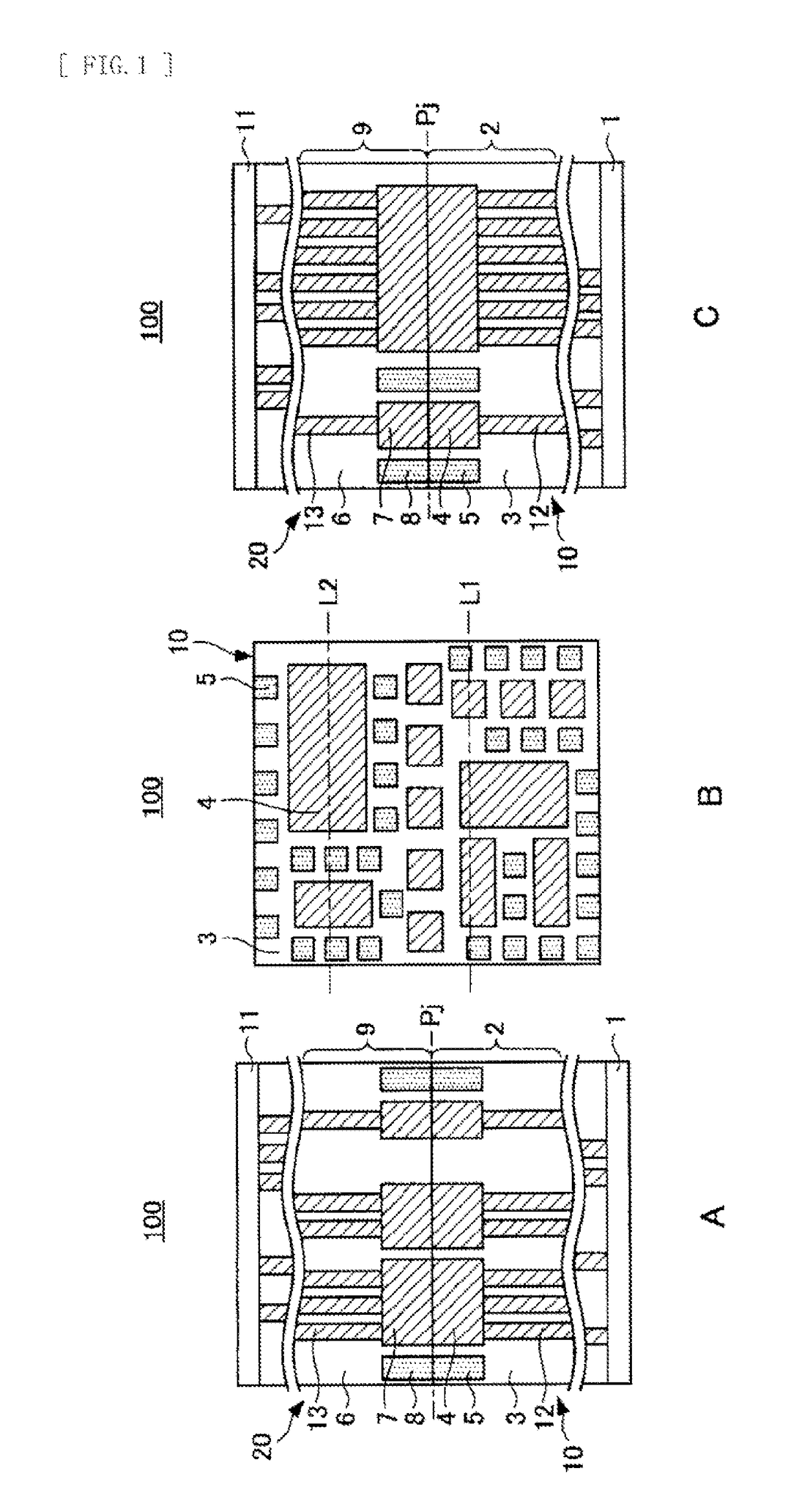
[0046]FIG. 1A is a schematic sectional view of a semiconductor device 100 according to a first embodiment. The semiconductor device 100 according to this embodiment includes a first semiconductor member 10 and a second semiconductor member 20 bonded to the first semiconductor member 10. Moreover, FIG. 1B is a diagram illustrating a bonding surface of the first semiconductor member 10, and FIG. 1A is a sectional view taken along a line L1 of FIG. 1B. Further, FIG. 1C is a sectional view taken along a line L2 of FIG. 1B.
[0047]As illustrated in FIGS. 1A and 1C, the first semiconductor member 10 includes, for example, a substrate 1 and a first wiring layer 2 formed on the substrate 1. Moreover, although not illustrated, for example, a semiconductor element such as a transistor or a diode is formed on the substrate 1. For example, a planarization film made of SiO2, NSG (nondoped silicate glass), PSG (phospho-silicate glass), or TEOS (tetraethoxysilane) is disposed on the semiconductor el...
second embodiment
[0059]In the first embodiment, the first electrode pads 4 and the second electrode pads 7, and the dummy electrode 5 and the dummy electrode 8 are disposed plane-symmetrically with respect to the bonding surface Pj. However, as described above, they are not necessarily disposed plane-symmetrically.
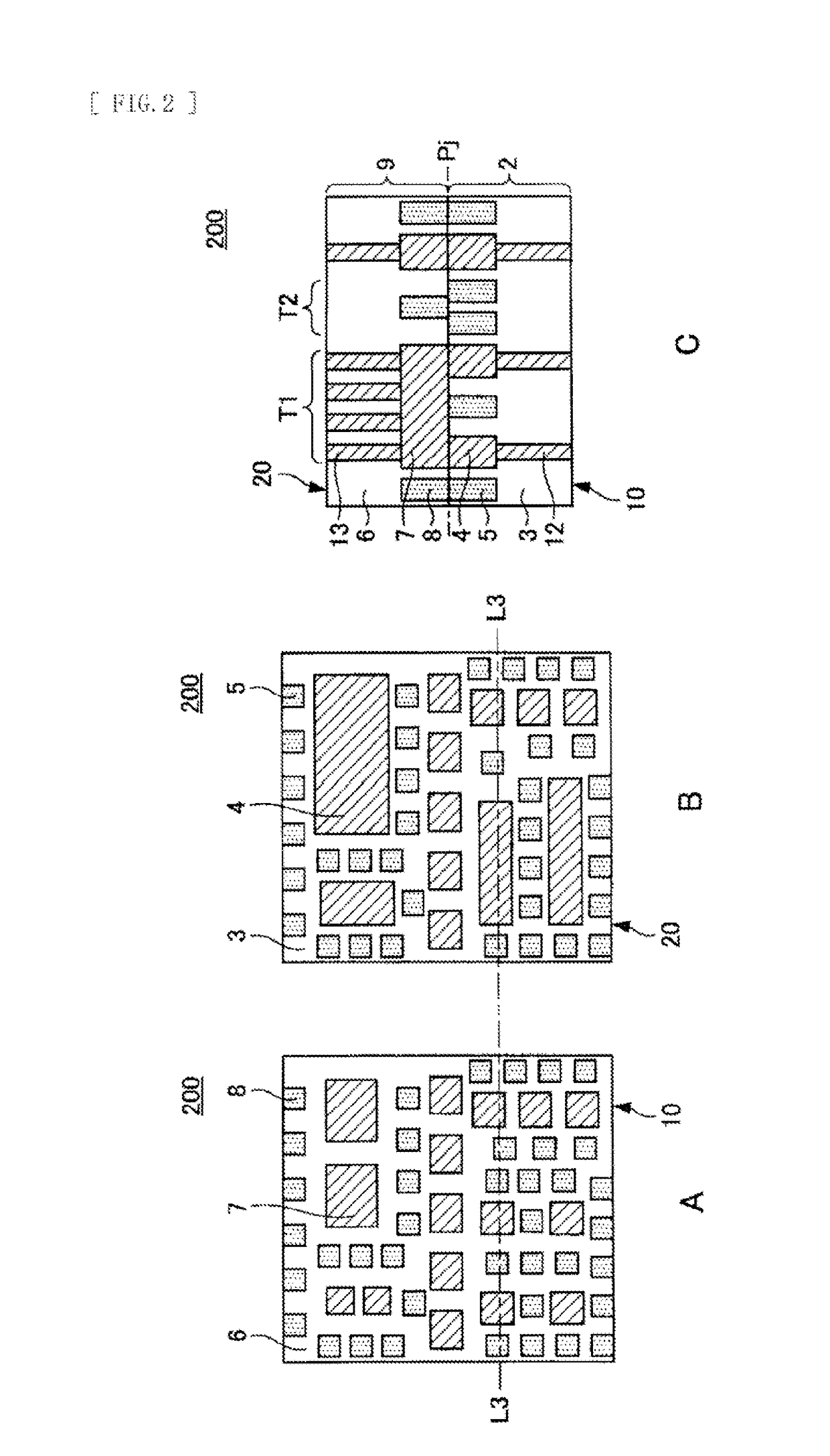
[0060]FIG. 2A is a diagram illustrating a bonding surface of the first semiconductor member 10 of a semiconductor device 200 according to a second embodiment and FIG. 2B is a diagram illustrating a bonding surface of the second semiconductor member 20. Moreover, FIG. 2C is a sectional view of the semiconductor device 200 taken along a line L3 illustrated in FIGS. 2A and 2B. It is to be noted that like components are denoted by like numerals as of the first embodiment, and will not be further described. Moreover, in this embodiment, configurations other than the first wiring layer 2 and the second wiring layer 9 are the same as those in the first embodiment (refer to FIG. 1C); therefore, in...
third embodiment
[0064]FIG. 3A is a diagram illustrating a bonding surface of the first semiconductor member 10 of a semiconductor device 300 according to a third embodiment, and FIG. 3B is a sectional view of the semiconductor device 300 taken along a line L4 illustrated in FIG. 3A. Moreover, in this embodiment, configurations other than the first wiring layer 2, the second wiring layer 9, a third wiring layer 18, and a fourth wiring layer 19 are the same as those in the first embodiment (refer to FIG. 1C); therefore, only these wiring layers are illustrated in FIG. 3B.
[0065]The semiconductor device 300 according to this embodiment includes the first semiconductor member 10 and the second semiconductor member 20. The first semiconductor member 10 includes the first wiring layer 2 and the third wiring layer 18. As illustrated in FIG. 3A, in this embodiment, the first electrode pads 4 and the dummy electrodes 5 in the first wiring layer 2 have the same bonding surface shape, and are all arranged at e...
PUM
 Abstract
Description
Claims
Application Information