High output power light emitting device and packaged used therefor

a technology of light emitting device and high output power, which is applied in the manufacture of semiconductor/solid-state devices, semiconductor devices, electrical apparatus, etc., can solve the problems of increasing the possibility of ag film peeling off the lead electrode, and achieve the effects of improving the efficiency of dissipating heat, reducing the bonding strength, and increasing the bonding strength

Active Publication Date: 2009-10-22
NICHIA CORP
View PDF24 Cites 104 Cited by
  • Summary
  • Abstract
  • Description
  • Claims
  • Application Information

AI Technical Summary

Benefits of technology

[0010]Accordingly, an object of the present invention is to provide a light emitting device that has high output power and long service life where a package is suppressed from discoloring due to heat generation.
[0013]When the thickness of the Ag film is larger than 20 μm, the Ag film becomes more likely to peel off due to thermal stress during bonding of the light emitting element with a soldering material or mounting the light emitting device on a circuit board. That is, when the Ag film is thicker, the Ag film undergoes greater thermal expansion or shrinkage when mounting the light emitting element with a soldering material, thus increasing the possibility of the Ag film peeling off the lead electrode.
[0014]According to the present invention, the Ag film that has high crystallinity and high density and is less likely to discolor is obtained by controlling the thickness of the Ag film to 0.5 μm or larger. As a result, the Ag film is suppressed from absorbing light, and heat generated in the package is decreased. On the other hand, the Ag film is suppressed from peeling off by controlling the thickness of the Ag film to 20 μm or less, while maintaining a sufficient contact area between the Ag film and the eutectic layer. As a result, heat generated by the light emitting element is transferred efficiently through the eutectic layer to the lead electrode, thus improving the heat dissipation of the light emitting device. There is also such an effect achieved as the strength of bonding between the light emitting element and the lead electrode is increased so that failure rate of the light emitting element can be reduced.
[0018]When the flatness of the Ag film is less than 0.001 μm, on the other hand, the Ag film that is too smooth does not provide tiny surface irregularities whereon the eutectic layer is to be anchored. As a result, peel-off becomes more likely to occur between the eutectic layer and the Ag film, thus leading to a decrease in the bonding strength.
[0019]According to the present invention, flatness of the Ag film (namely the flatness of the surface of the lead electrode that is covered by the Ag film) is controlled in a range from 0.001 to 50 μm, thereby improving the efficiency of dissipating heat generated by the light emitting element, and increasing the bonding strength between the light emitting element and the lead frame, thus achieving an effect of reducing the failure rate of the light emitting device.
[0020]According to the present invention, as described above, heat buildup in the light emitting device can be mitigated and the package can be suppressed from discoloring, so that the light emitting device of high output power and long service life can be made. Moreover, according to the present invention, bonding strength between the light emitting element and the lead frame can be increased and therefore failure rate of the light emitting device can be reduced.

Problems solved by technology

That is, when the Ag film is thicker, the Ag film undergoes greater thermal expansion or shrinkage when mounting the light emitting element with a soldering material, thus increasing the possibility of the Ag film peeling off the lead electrode.

Method used


Image

  • High output power light emitting device and packaged used therefor
  • High output power light emitting device and packaged used therefor
  • High output power light emitting device and packaged used therefor

Examples


first embodiment

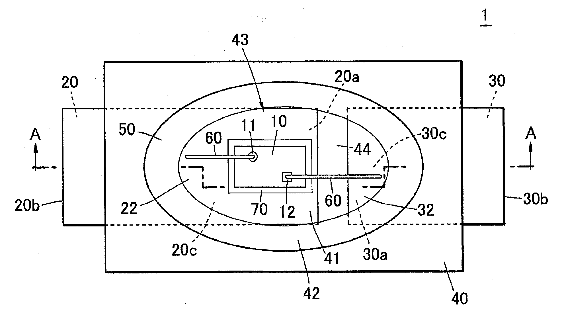
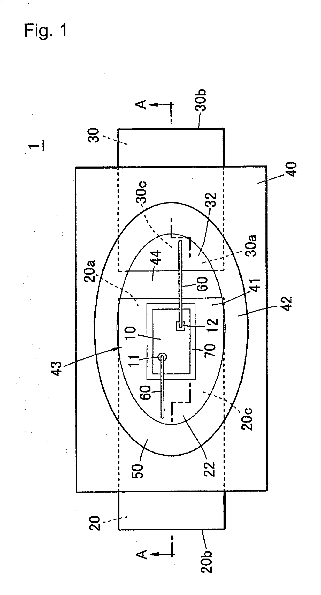
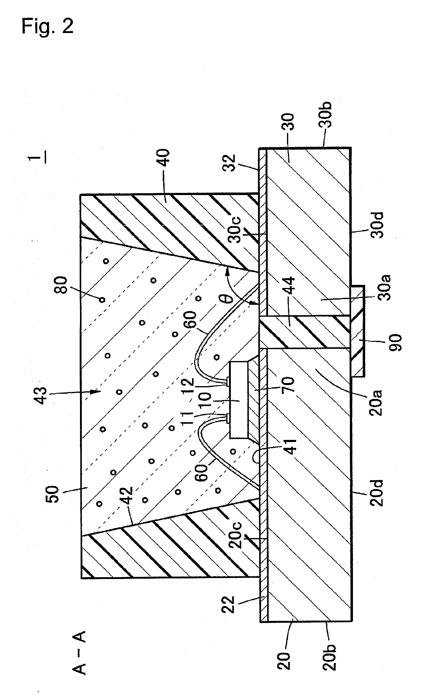
[0029]The light emitting device 1 of this embodiment shown in FIG. 1 and FIG. 2 comprises a light emitting element 10, a package 40 having a recess 43 to mount the light emitting element 10 thereon, and a sealing member 50 that covers the light emitting element 10.

[0030]The package 40 has two lead electrodes (a first lead electrode 20 and a second lead electrode 30) fixed thereon, and surfaces of ends of the lead electrodes 20, 30 on one side thereof (inner lead sections 20a, 30a) are exposed at the bottom 41 of the recess 43.

[0031]Ends of the lead electrodes 20, 30 on the other side thereof (outer lead sections 20b, 30b) protrude to the outside of the package 40.

[0032]The light emitting element 10 is mounted in the recess 43 of the package 40 through a eutectic layer 70 on an upper surface 20c of the inner lead 20a of the first lad electrode 20. The light emitting element 10 shown is such a type as two electrodes 11, 12 are formed on the surface thereof, where the first electrode 1...

example 1

Examples 1 to 10


PUM


Abstract

An object of the present invention is to provide a light emitting device that has high output power and long service life where a package is suppressed from discoloring due to heat generation. The light emitting device 1 of the present invention contains a light emitting element 10, a package 40 formed of a thermosetting resin, the package having a recess 43 wherein the light emitting element 10 is mounted, a first lead electrode 20 which is exposed at the bottom of the recess 43 of the package 40 and whereon the light emitting element 10 is mounted, and a second lead electrode 30 which is exposed at the bottom of the recess 43 of the package 40 and is electrically connected to the light emitting element 10. The light emitting element 10 is bonded to the first lead electrode 20 through a eutectic layer 70, and at least a surface of the first electrode 20 is coated with an Ag film 22, a thickness of the Ag film 22 being in the range from 0.5 μm to 20 μm.

Description

BACKGROUND OF THE INVENTION[0001]1. Field of the Invention[0002]The present invention relates to a surface-mounted light emitting device used in lighting apparatus, display, backlight light source for cell phone, auxiliary light source for moving picture and other light sources for general use, and resin molding suitable for the same.[0003]2. Description of the Related Art[0004]Surface-mounted light emitting devices based on the light emitting element are small in size, high in power efficiency and are capable of emitting light of clear colors. The light emitting element that is a semiconductor element is also free of failure such as burnout. Moreover, the light emitting element has such advantages as excellent startup characteristic and high durability to vibration and to repetitive operations of turning ON / OFF. Because of such excellent characteristics, the light emitting devices based on light emitting elements such as light emitting diode (LED) and laser diode (LD) are used in v...

Claims


Application Information

Patent Timeline
Patent Type & Authority Applications(United States)
IPC IPC(8): H01L33/00H01L21/50H01L33/60H01L33/62H01L33/64
CPCH01L33/60H01L2224/45015H01L33/647H01L2224/48091H01L2224/48465H01L2224/73265H01L33/62H01L24/45H01L2924/3025H01L2224/45144H01L2224/48227H01L2224/32225H01L2924/01322H01L2924/01066H01L2924/01019H01L2924/00014H01L2924/00H01L2924/00012H01L2924/12035H01L2924/12036H01L2924/12041H01L24/73H01L2924/181H01L2224/05554H01L2924/20753
Inventor HAYASHI, MASAKI
Owner NICHIA CORP
Why Eureka
Try Eureka