Textured phosphor conversion layer light emitting diode

a technology of light-emitting diodes and phosphors, which is applied in the direction of basic electric elements, electrical apparatus, and semiconductor devices, can solve the problems of non-uniform and typically decrease in overall luminous efficiency, and inability to apply phosphor uniformly and typically. uniform and smooth application of phosphor, etc., to achieve the effect of increasing the total luminous efficacy of the device and high light extraction efficiency

Active Publication Date: 2014-10-14
RGT UNIV OF CALIFORNIA
View PDF132 Cites 80 Cited by
  • Summary
  • Abstract
  • Description
  • Claims
  • Application Information

AI Technical Summary

Benefits of technology

[0029]The present invention describes an (Al, Ga, In)N and light emitting diode (LED) combined with a textured, or shaped, phosphor conversion in which the multi directions of light can be extracted from the surfaces of the chip and phosphor layer before subsequently being extracted to air. The present invention combines the high light extraction efficiency LED chip with shaped (textured) phosphor layers to increase the total luminous efficacy of the device. As a result, this combined structure extracts more light out of the white LED.
[0030]The present invention minimizes the internal reflection of the phosphor layer by preferential patterning the emitting surface to direct more light away from the absorbing chip structure. In order to minimize the internal reflection of the LED light further, transparent electrode such as Indium Tin Oxide (ITO) or Zinc Oxide (ZnO), or the surface roughening of AlInGaN by patterning or anisotropically etching, or the roughening of ITO and ZnO, or the roughening of epoxy and glass or the roughening of the phosphor layer, are used. The present invention furthermore combines the high light extraction efficiency LED chip with shaped (textured) phosphor layers to increase the total luminous efficacy of the device. As a result, this combined structure extracts more light out of the LED.
[0031]More particularly the invention relates to (Al, Ga, In)N LEDs and light extraction structure combined with phosphors and optimized optics for highly efficient (Al, Ga, In)N based light emitting diodes applications, and its fabrication method. Present invention describes a white high efficient LED created by maximizing extraction from the photon conversion layer. In the present invention it has been shown that roughening the surface of a phosphor layer increases the luminous efficacy of a white LED. In order to roughen the phosphor layer the phosphor is first prepared in a resin mixture. It is then poured directly onto an aluminum oxide 120-grit square piece of sandpaper (120 abrasive particles per inch). The optic used for the remote phosphor layer is then placed on top of the phosphor. This serves to flatten the phosphor on the sandpaper so that a thin uniform layer is produced. These items are then heated under the curing conditions for the resin.
[0032]A further extension is the general combination of a shaped high refractive index light extraction material with transparent conducting electrodes, textured phosphor conversion layers and shaped optical elements. The overall effect is to achieve a device with superior luminous efficacy and a high output power.

Problems solved by technology

This results in a decrease in overall luminous efficiency.
Previous applications of the phosphor conversion layer are limited to placing a gel or other liquid form of material onto the chip, and allowing the phosphor to cure.
This non-uniform and typically smooth application of the phosphor does not take into account several factors that can be used to increase the efficiency of the LED.

Method used


Image

  • Textured phosphor conversion layer light emitting diode
  • Textured phosphor conversion layer light emitting diode
  • Textured phosphor conversion layer light emitting diode

Examples


Embodiment Construction

[0055]In the following description of the preferred embodiment, reference is made to the accompanying drawings which form a part hereof, and in which is shown by way of illustration a specific embodiment in which the invention may be practiced. It is to be understood that other embodiments may be utilized and structural changes may be made without departing from the scope of the present invention.

[0056]Overview

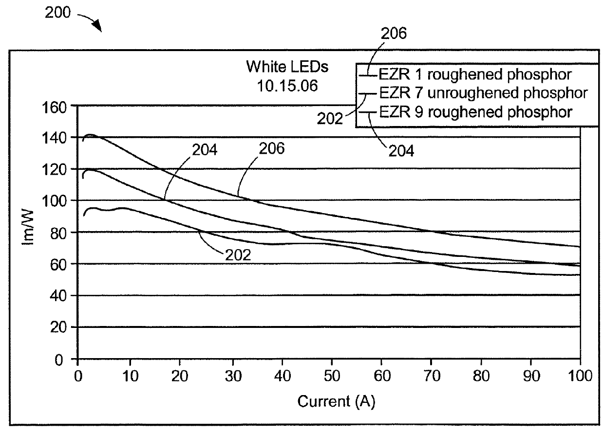
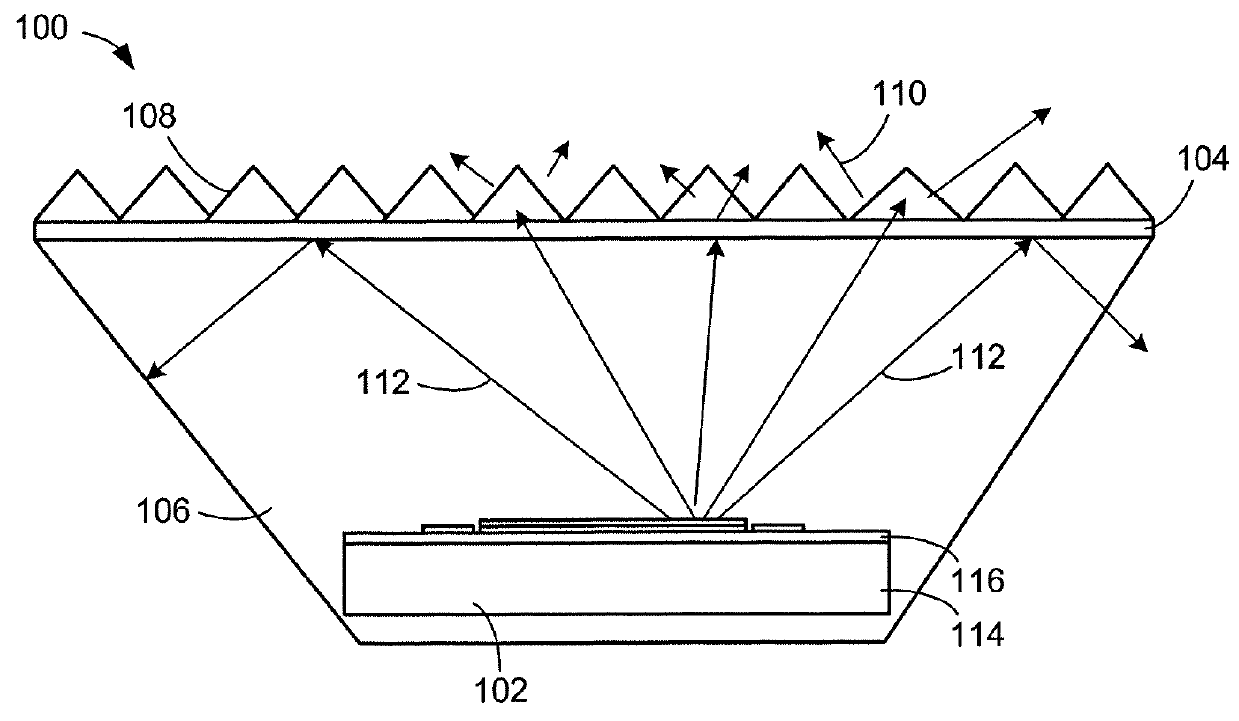
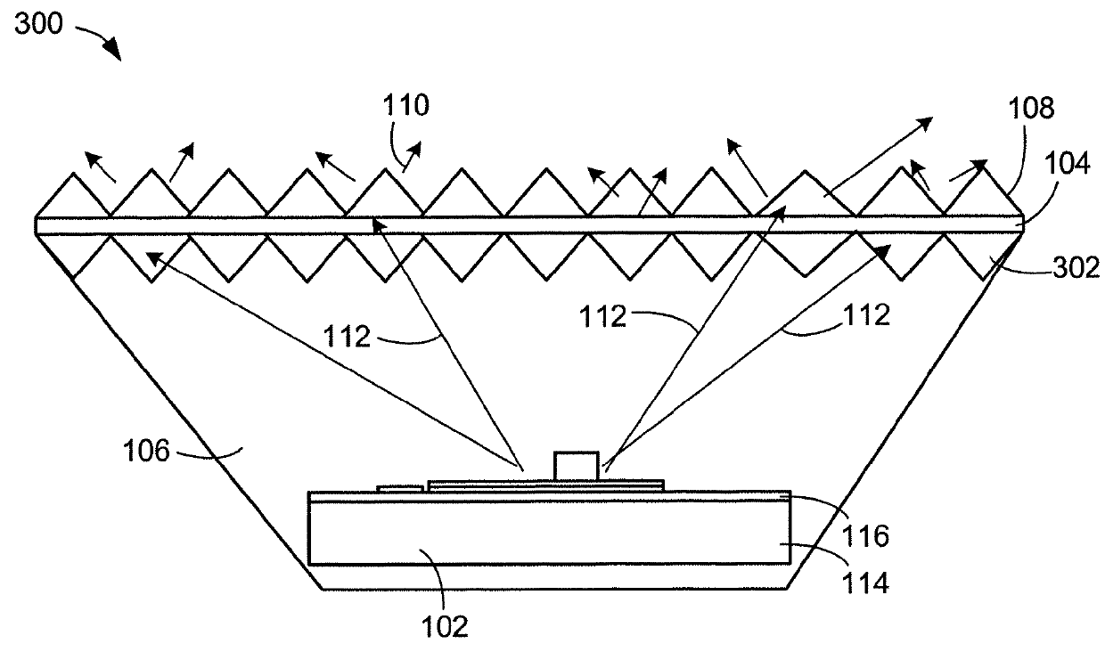
[0057]The present invention describes the high efficient LEDs which use the phosphor to change the emission color of the LEDs. FIG. 1 shows the structure of the white LEDs which utilize the phosphor to get the white emission color. The phosphor layer is located near the surface of the inverted cone shape epoxy molding. When the surface of the phosphor layer is roughened, the luminous efficacy of the white LEDs is increased as shown in FIG. 2 in comparison with the white LEDs with a flat surface of the phosphor layer. The surface roughening improves the light extraction efficie...


PUM


Abstract

This invention is related to LED Light Extraction for optoelectronic applications. More particularly the invention relates to (Al, Ga, In)N combined with optimized optics and phosphor layer for highly efficient (Al, Ga, In)N based light emitting diodes applications, and its fabrication method. A further extension is the general combination of a shaped high refractive index light extraction material combined with a shaped optical element.

Description

CROSS-REFERENCE TO RELATED APPLICATIONS[0001]This application is related to the following commonly-assigned applications:[0002]U.S. Utility application Ser. No. 10 / 581,940, filed on Jun. 7, 2006, by Tetsuo Fujii, Yan Gao, Evelyn. L. Hu, and Shuji Nakamura, entitled “HIGHLY EFFICIENT GALLIUM NITRIDE BASED LIGHT EMITTING DIODES VIA SURFACE ROUGHENING,” now U.S. Pat. No. 7,704,763, issued Apr. 27, 2010, which application claims the benefit under 35 U.S.C Section 365(c) of PCT Application Serial No. US2003 / 03921, filed on Dec. 9, 2003, by Tetsuo Fujii, Yan Gao, Evelyn L. Hu, and Shuji Nakamura, entitled “HIGHLY EFFICIENT GALLIUM NITRIDE BASED LIGHT EMITTING DIODES VIA SURFACE ROUGHENING;”[0003]U.S. Utility application Ser. No. 11 / 054,271, filed on Feb. 9, 2005, by Rajat Sharma, P. Morgan Pattison, John F. Kaeding, and Shuji Nakamura, entitled “SEMICONDUCTOR LIGHT EMITTING DEVICE,” now U.S. Pat. No. 8,227,820 issued Jul. 24, 2012;[0004]U.S. Utility application Ser. No. 11 / 175,761, filed ...

Claims


Application Information

Patent Timeline
Patent Type & Authority Patents(United States)
IPC IPC(8): H01L33/22H01L33/44H01L33/50H01L33/58
CPCH01L33/22H01L33/44H01L33/508H01L33/58H01L2933/0091H01L33/507H01L33/505H01L33/0075H01L33/32H01L33/62H01L2224/48091H01L2224/73265H01L2933/0041H01L2933/0066H01L33/06H01L33/145H01L33/502H01L33/60H01L2224/49107H01L2924/181H01L2933/0058
Inventor FELLOWS, NATALIE N.DENBAARS, STEVEN P.NAKAMURA, SHUJI
Owner RGT UNIV OF CALIFORNIA
Why Eureka
Try Eureka