

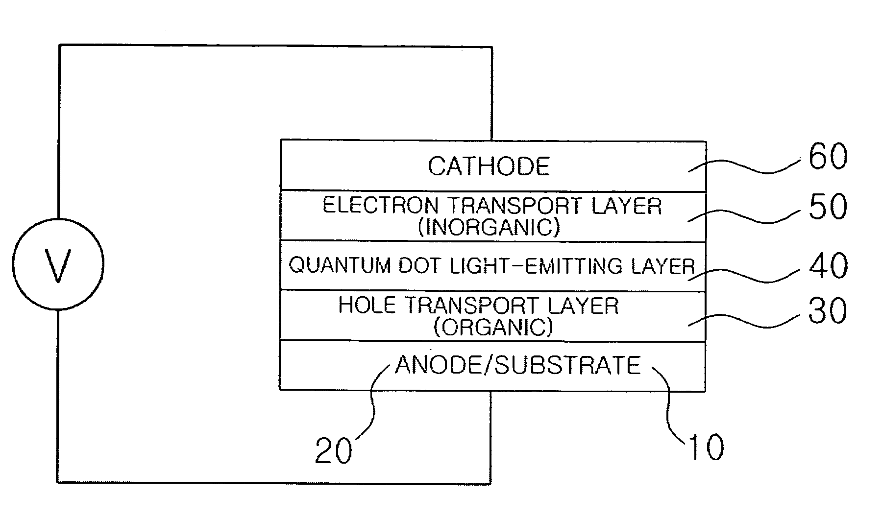
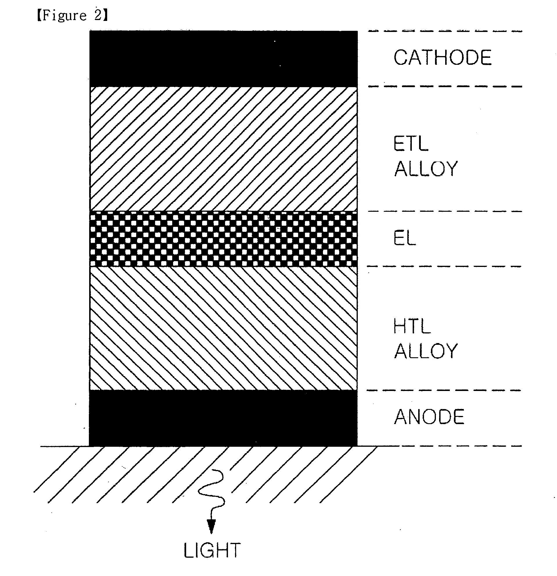
Quantum Dot Light-Emitting Diode Comprising Inorganic Electron Transport Layer
- Summary
- Abstract
- Description
- Claims
- Application Information
AI Technical Summary
Benefits of technology
Problems solved by technology
Method used
Image

Examples
example 1
Fabrication of Quantum Dot Light-Emitting Diode
[0032]A glass substrate on which ITO was patterned was sequentially washed with a neutral detergent, deionized water, water and isopropyl alcohol, and then the resulting substrate was treated with UV-ozone. A hole transport layer and a quantum dot thin film were sequentially formed on the ITO substrate. Specifically, (N,N′-diphenyl-N,N′-bis(3-methylphenyl)-(1,1′-biphenyl)-4,4′-diamine (TPD) was dissolved in chloroform to prepare a solution (1 wt %). Separately, the CdS quantum dots prepared in Preparative Example 1 were dispersed in chloroform to prepare a dispersion (1 wt %). The TPD solution and the CdS dispersion were mixed in a ratio of 1:1. The resulting solution was spin-coated on the ITO substrate at about 2,000 rpm for one minute and dried to form a TPD / quantum dot thin film having a thickness of about 45 nm.
[0033]*44TiO2 was coated to a thickness of 40 nm on top of the dried quantum dot light-emitting layer by e-beam evaporatio...
example 2
Fabrication of Quantum Dot Light-Emitting Diode
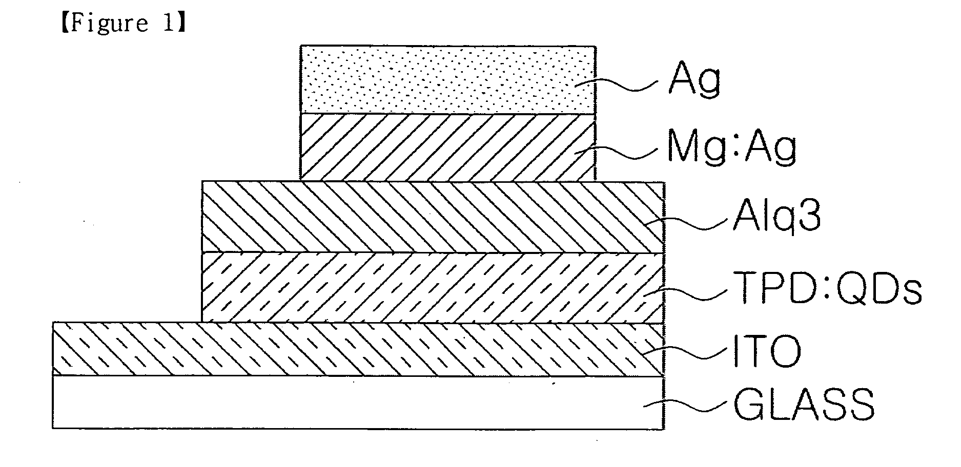
[0035]A TiO2 precursor sol (DuPont Tyzor, BTP, 2.5 wt % in buthanol) was spin-coated on a patterned ITO cathode at 2,000 rpm under a nitrogen atmosphere for 30 seconds, dried under a nitrogen atmosphere for 5 minutes, and annealed at 150° C. for 15 minutes to form an amorphous TiO2 thin film having a thickness of about 20 nm. A solution (0.3 wt %) of red CdSe / ZnS core / shell structured nanocrystals (Evidot 630 nm absorbance) (Evidot Red (CdSe / ZnS), Evident Technology) was spin-coated on the TiO2 thin film at 2,000 rpm for 30 seconds, and dried at 50° C. for 5 minutes. N,N′-di(naphthalen-1-yl)-N-N′-diphenyl-benzidine (NPB) was deposited to a thickness of about 40 nm on the quantum dot light-emitting layer using a thermal evaporator in a glove box to form an organic thin film. Finally, Au was deposited to a thickness of 100 nm using a patterned mask to form an electrode, completing the fabrication of a quantum dot light-emitting diode. The...
PUM
| Property | Measurement | Unit |
|---|---|---|
| Electrical resistance | aaaaa | aaaaa |
| Efficiency | aaaaa | aaaaa |
| Velocity | aaaaa | aaaaa |
Abstract
Description
Claims
Application Information