Semiconductor device

a technology of semiconductors and thin films, applied in the direction of semiconductor lasers, semiconductor/solid-state device details, transistors, etc., can solve the problems of large mismatch between zno and the thin film material of the semiconductor, difficult to form a high-quality single crystal thin film, etc., to improve the performance of the heterostructured device, reduce the gate voltage for switching, and improve the effect of heterostructur

Inactive Publication Date: 2005-04-12
JAPAN SCI & TECH CORP
View PDF7 Cites 109 Cited by
  • Summary
  • Abstract
  • Description
  • Claims
  • Application Information

AI Technical Summary

Benefits of technology

According to the invention, an object is to manufacture a transparent semiconductor device by combining a transparent semiconductor material of ZnO with a transparent and highly insulating SCAM substrate, and greatly improve the performance of a heterostructured device.
An object is to achieve a high switching speed by applying the invention to a transistor or the like. In addition, an object is to lower a gate voltage for switching by applying the invention to a field effect transistor so as to obtain a wider depletion layer when an electric field is applied. Another object is to increase light emission efficiency by applying the invention to a light emission device.
An object is to improve the performance of various electron devices by applying the invention to the devices including a field effect transistor, a bipolar transistor, a light emission device containing a GaN based nitride blue laser (LED, laser), a surface acoustic wave (SAW) device, a sensor or the like.

Problems solved by technology

However, in the conventional substrate using sapphire or the like, lattice mismatching with ZnO as a thin film material was large, reaching ap roximately 18%.
Consequently, a grain boundary existed or mosaicness was increased to make it difficult to form a high quality single crystal thin film.
In addition, conventionally, with regard to device performance, the intrinsic performance of ZnO was not placed into full play, making it impossible to always manufaccure an optimal substrate.

Method used


Image

  • Semiconductor device
  • Semiconductor device
  • Semiconductor device

Examples


first embodiment

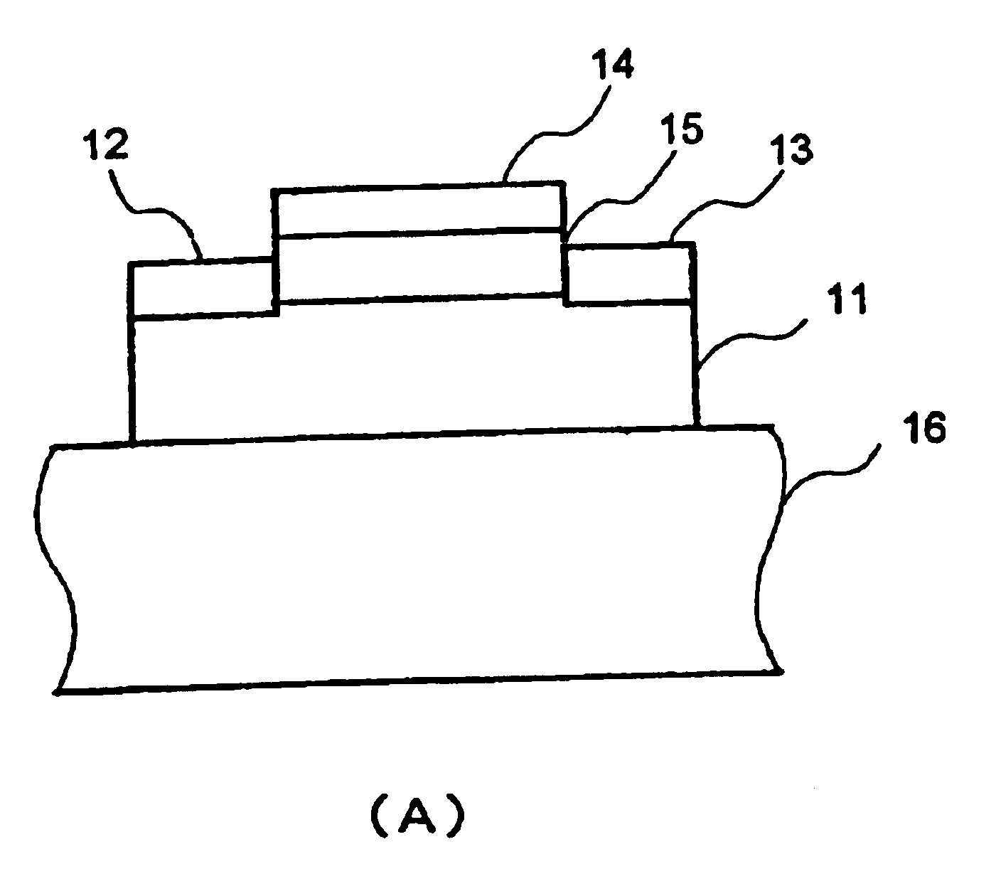
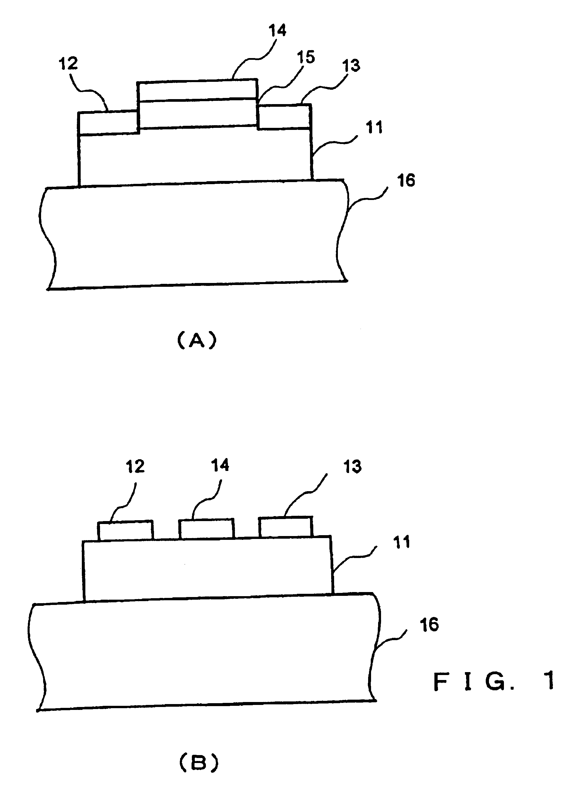
FIG. 1B specifically shows a modified example of the This transistor includes the channel layer 11 formed on the substrate 16. Further, on the channel layer 11, the source 12 and the drain 13 are formed by ohmic junction, and the gate 14 is formed by Schottky junction. In this example, since the gate insulating layer 15 does not exist unlike the case shown in FIG. 1A, proper spacing is set between the source 12 / drain 13 and the gate 14.

Next, description will be made of materials for components, which are the main features of the invention.

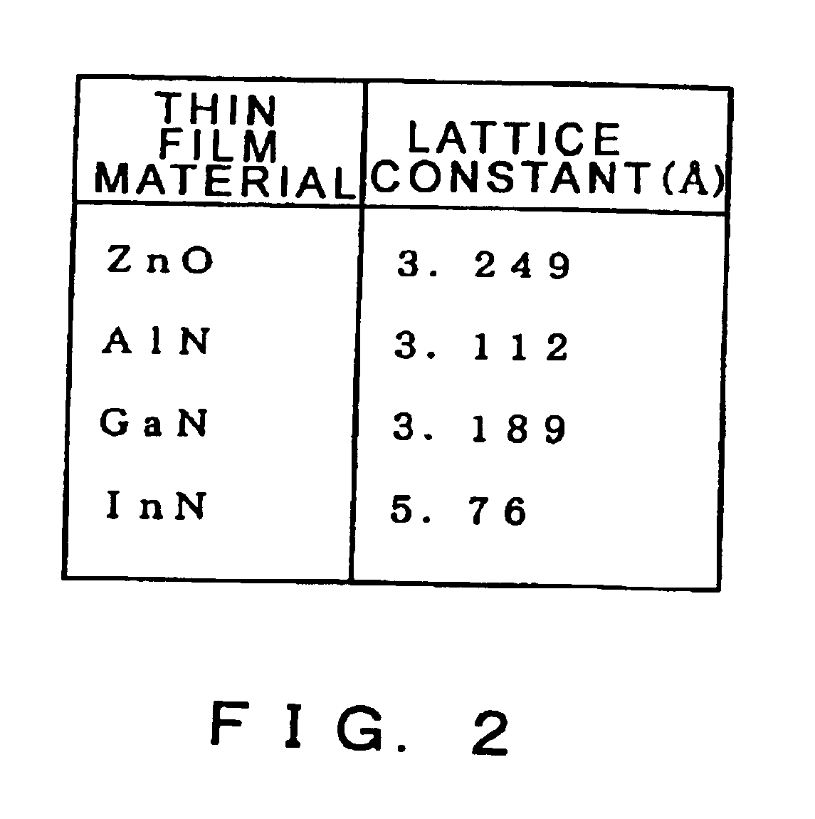
First, the channel layer 11 is formed of a proper conductive or insulating semiconductor based on an FET structure. As a material to be used for the channel layer 11, other than a widely known semiconductor material, one can be selected from group II oxides including, e.g., zinc oxide ZnO, zinc magnesium oxide MgxZn1−xO, zinc cadmium oxide CdxZn1−xO, cadmium oxide CdO, and so on. For the channel layer 11, one selected from group III nitrides inclu...

second embodiment

If the channel layer 11 is in an undoped pure state, or slightly doped with impurities, a constitution like that shown in FIG. 1A is employed to realizing good compatibility between the lattice constants of the substrate 16 and the channel layer 11. On the other hand, with regard to a case where a material doped with a considerable amount of impurities (e.g., about 10 to 20%) is used for the channel layer 17, or the like, the compatibility between the lattice constants can be further improved. Here, for such a purpose, the buffer layer 18 is provided between the substrate 16 and the channel layer 17.

For the channel layer 17, a material having a composition similar to that of the first embodiment. However, in the second embodiment, one doped with relatively large amount of impurities can be used. For the substrate 16, similarly to the case of the first embodiment, a material having high compatibility is used properly according to the channel layer 17. For the buffer layer 18, if gro...

third embodiment

FIG. 12B shows a modified example of the Different from the one shown in FIG. 12A, the gate insulating layer 25 is not formed, and the gate 24 and the channel layer 21 are coupled by Schottky junction. If the gate insulating layer 25 is formed as in the case shown in FIG. 12A, there is little limitation placed on a voltage applied to the gate. On the other hand, if the gate insulating layer 25 is not formed as in the case shown in FIG. 12B, a withstand voltage is lowered between the gate and the source, and between the gate and the drain. In this case, a manufacturing process is simple.

With such constitutions, as described above with reference to the first and second embodiments, the thin film material of the channel layer 21, the source 22 or the drain 23, and the material of the substrate 26 or the gate insulating layer 25 can be properly combined to be used so that the lattice constants of both can be matched with each other.

FIG. 13 is a sectional view showing a semiconductor de...


PUM

PropertyMeasurementUnit
temperaturesaaaaaaaaaa
semiconductoraaaaaaaaaa
structureaaaaaaaaaa

Abstract

The present invention provides a high quality thin film comparable to a bulk single crystal and providres a semiconductor device with superior characteristics. A channel layer 11, for example, is formed of a semiconductor such as zinc oxide ZnO or the like. A source 12, a drain 13, a gate 14 and a gate insulating layer 15 are formed on the channel layer 111 to form an FET. For a substrate 16, a proper material is selected depending on a thin film material of the channel layer 11 in consideration of compatibility of both lattice constants. For example, if ZnO is used for the semiconductor of the channel layer as a base material, ScAlMgO4 or the like can be used for the substrate 16.

Description

TECHNICAL FIELDThe present invention relates to a semiconductor device. More particularly, the invention relates to a semiconductor device having a high quality single crystal thin film formed by using group II oxide or group III nitride as a thin film material, and an oxide single crystal having good lattice compatibility with the thin film material for a substrate. The invention also relates to the application of such a semiconductor device to a light emission device, a surface acoustic wave (SAW) device, or the like.BACKGROUND ARTHeretofore, in the semiconductor device, for example, as a transistor, a thin film transistor using amorphous silicon, polycrystal silicon or the like has been utilized. Recently, focus of attention has been placed on zinc oxide (ZnO) to be used as a thin film material for manufacturing the semiconductor device. Not only an ultraviolet ray emission device, a transparent transistor, and so on, have replaced the existing application as photo-electron devic...

Claims


Application Information

Patent Timeline
Patent Type & Authority Patents(United States)
IPC IPC(8): C01G1/02H01L21/36H01L29/66H01L21/02H01L29/22H01L29/02H01L29/786H01S5/347H01S5/32H01S5/00H01L21/338H01L27/15H01L29/12H01L29/812H01L33/06H01L33/10H01L33/12H01L33/20H01L33/28H01L33/32H01L33/40H01L33/46
CPCB82Y20/00H01L21/02565H01L29/22H01L29/78603H01L29/7869H01L21/0242H01L21/02472H01L21/02488H01L21/02502H01L21/0254H01L21/02554C01G1/02C01P2002/77H01S5/3214H01S5/347H01L29/45H01L29/4908H01L21/84
Inventor KAWASAKI, MASASHIOHNO, HIDEOOHTOMO, AKIRA
Owner JAPAN SCI & TECH CORP
Why Eureka
Try Eureka