Method and structure reducing parasitic influences of deflection devices in an integrated spatial light modulator

a spatial light modulator and deflection device technology, applied in the field of semiconductor processing techniques, can solve the problems of time-consuming and expensive process, inability to meet the requirements of the application, and undesirable adhesion of the suspended member to the electrode, so as to reduce the dimensions of the composite substrate used in one embodiment, reduce cost, and relax the alignment tolerances used during the substrate bonding process

Active Publication Date: 2007-02-27
MIRADIA INC
View PDF72 Cites 110 Cited by
  • Summary
  • Abstract
  • Description
  • Claims
  • Application Information

AI Technical Summary

Benefits of technology

[0008]According to an embodiment of the present invention, a method of fabricating an integrated spatial light modulator with contact structures is provided. The method includes providing a first substrate having a bonding surface, providing a device substrate having a device surface, and depositing a first layer on the device surface, the first layer having an upper surface opposite the device surface. The method also includes patterning the first layer to define a plurality of contact structure openings passing through the first layer from the upper surface to the first substrate, depositing a conductive layer on the upper surface of the first layer, and reducing the thickness of the conductive layer. The method further includes removing at least a portion of the first layer to expose a plurality of contact structures, depositing a standoff layer on the first layer, the standoff layer having an upper surface opposite the first layer, forming standoff structures from the standoff layer, and joining the bonding surface of the first substrate to the standoff structures to form a bonded substrate structure.
[0011]Numerous benefits are achieved using the present invention over conventional techniques. For example, in an embodiment according to the present invention, the alignment tolerances used during the substrate bonding process are greatly relaxed. Moreover, the dimensions of the composite substrate used in one embodiment are reduced, decreasing cost and improving layer uniformity. This increased layer uniformity extends, for example, to the thickness of a micro-mirror layer present in the composite substrate. Additionally, standoffs fabricated according to embodiments of the present invention provide a bonding surface with decrease surface roughness, leading to an increase in bond strength.
[0012]Moreover, embodiments of the present invention provides a means to simplify fabrication of spatial light modulator components. Additionally, the present invention provides a flexible design that can be optimized to meet the needs of particular applications. For example, the size and position of landing posts may be modified depending on the design constraints presented by a given application. In addition, the flexibility of design extends to materials optimized for particular applications. In embodiments according to the present invention, complex coatings are not necessary to reduce parasitic forces present in the MEMS. In certain embodiments, the invention also provides a way of operating a MEMS device to overcome stiction forces. Depending upon the embodiment, one or more of these benefits may exist. These and other benefits have been described throughout the present specification and more particularly below.

Problems solved by technology

Some of these fabrication processes require alignment of the substrates prior to bonding, with tolerances on the order of microns, which may be a time consuming and expensive process.
These parasitic forces may be strong enough to overcome the restoring force, resulting in an undesirable adhesion of the suspended member to the electrode.
Unfortunately, these techniques also have limitations.
For example, some coatings are difficult to deposit on small components and can require complex deposition equipment.
Moreover, complex mechanical structures may have reliability and lifetime concerns.

Method used


Image

  • Method and structure reducing parasitic influences of deflection devices in an integrated spatial light modulator
  • Method and structure reducing parasitic influences of deflection devices in an integrated spatial light modulator
  • Method and structure reducing parasitic influences of deflection devices in an integrated spatial light modulator

Examples


Embodiment Construction

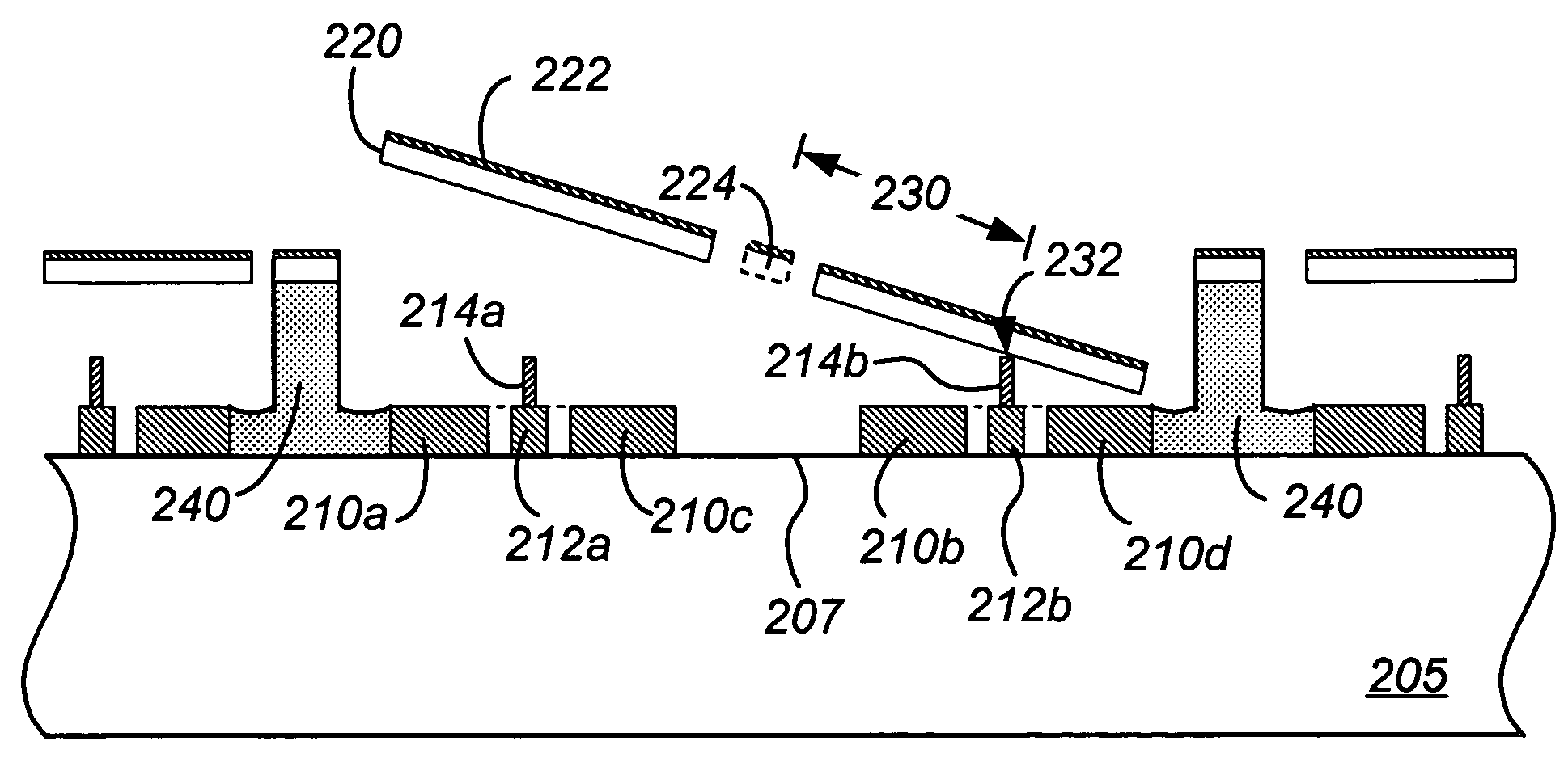
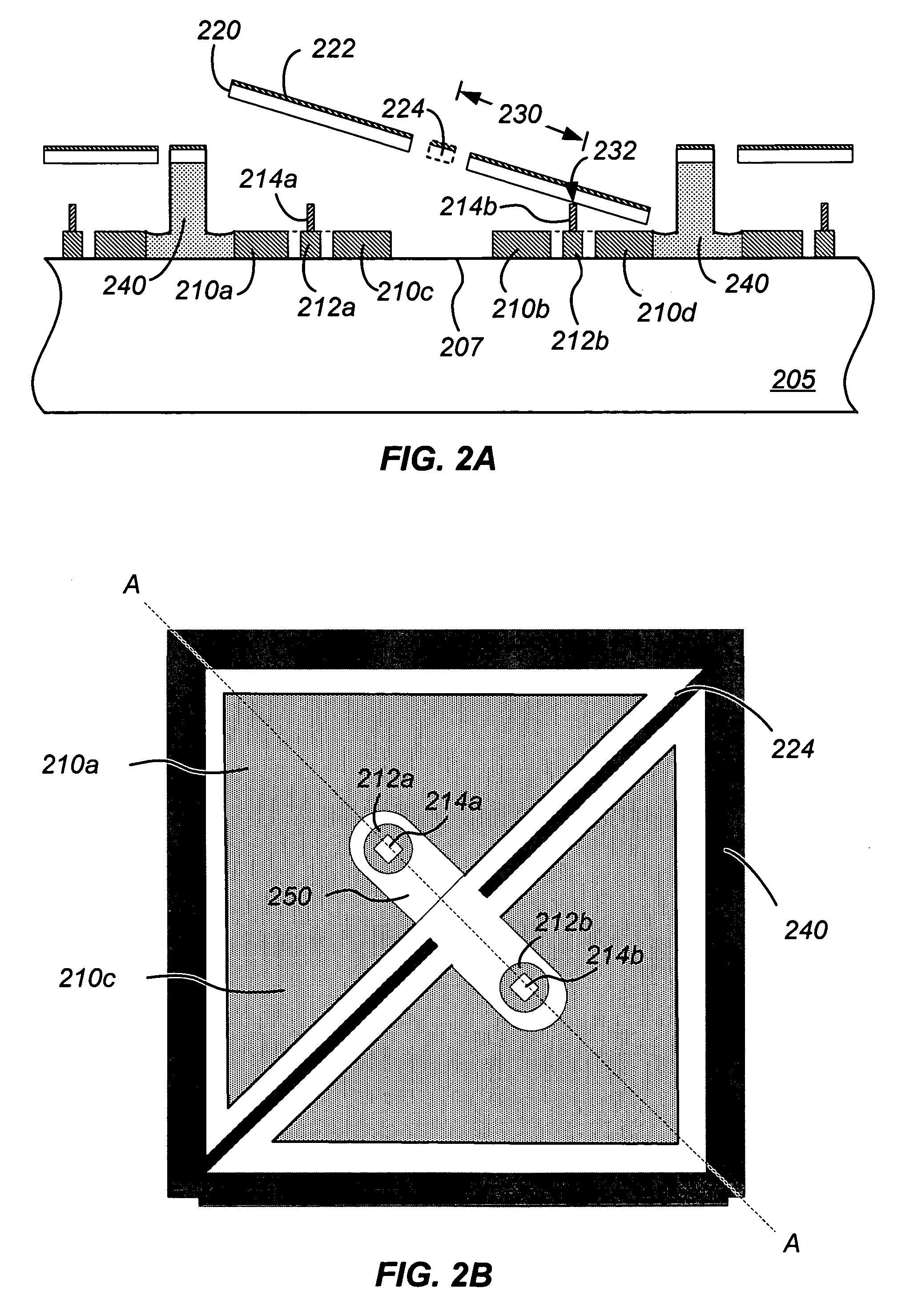
[0024]According to the present invention, techniques for semiconductor processing are provided. More particularly, the invention relates to a method and structure for forming an integrated spatial light modulator. Merely by way of example, the invention has been applied to a method of forming standoff structures in a bonded substrate structure and micro-electromechanical systems with reduced parasitic forces. The method and structure can be applied to other applications as well, such as actuators, sensors, detectors, and display components.

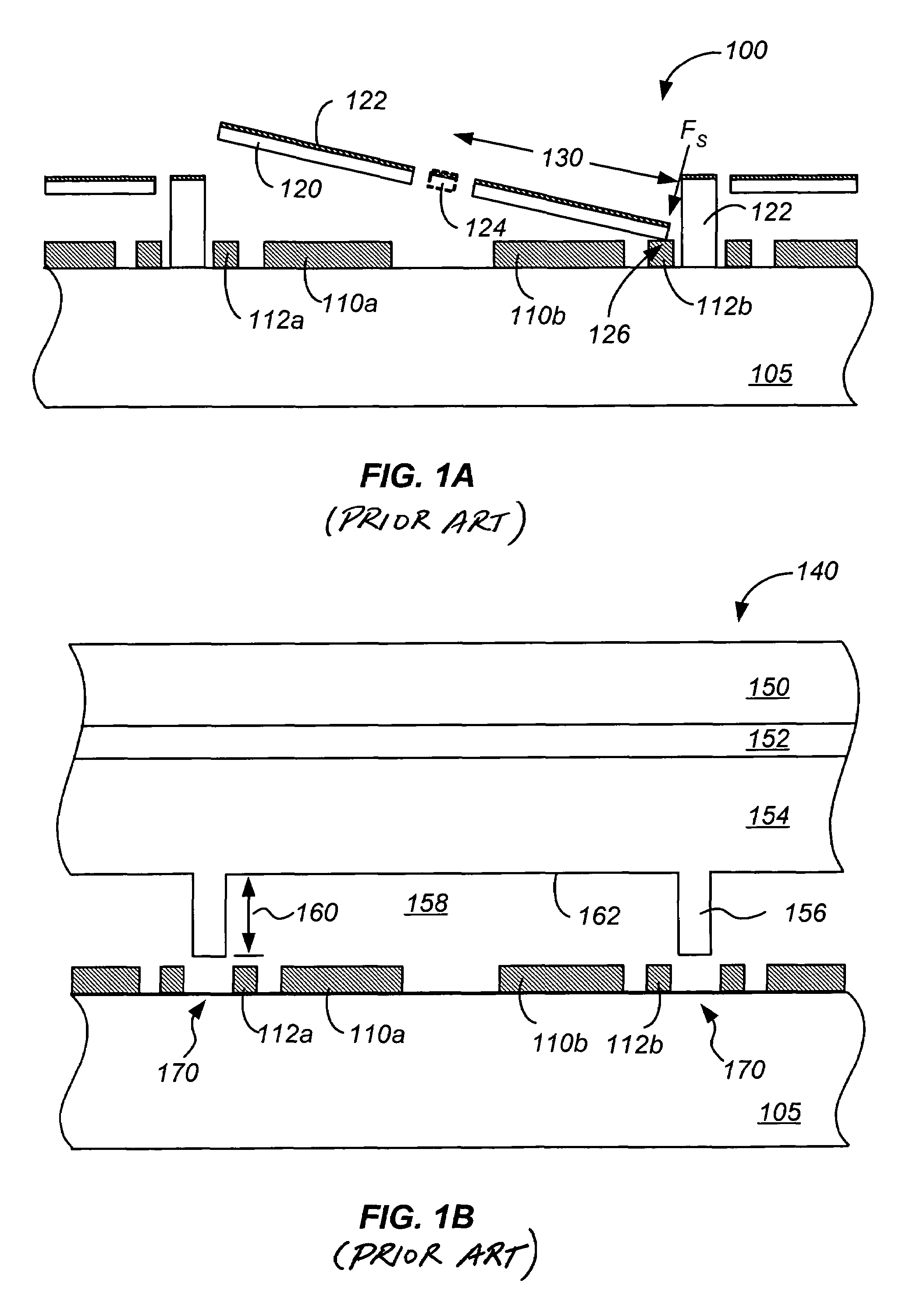
[0025]FIG. 1A is a simplified cross-sectional illustration of a conventional spatial light modulator. Suspended member 120 is suspended at a predetermined height above a substrate 105. Suspended member 120 has a reflective surface 122 coupled to the member. In addition, a torsion spring 124 is coupled to both the suspended member and a support structure (not shown) on substrate 105. In the figure, an electric potential has been applied between ele...


PUM


Abstract

A method of fabricating an integrated spatial light modulator with contact structures. The method includes providing a first substrate having a bonding surface, providing a device substrate having a device surface, and depositing a first layer on the device surface, the first layer having an upper surface opposite the device surface. The method also includes patterning the first layer to define a plurality of contact structure openings, depositing a conductive layer on the upper surface of the first layer, reducing the thickness of the conductive layer, and removing at least a portion of the first layer to expose a plurality of contact structures. The method further includes depositing a standoff layer on the first layer, forming standoff structures from the standoff layer, and joining the bonding surface of the first substrate to the standoff structures to form a bonded substrate structure.

Description

BACKGROUND OF THE INVENTION[0001]The present invention relates generally to semiconductor processing techniques. More particularly, the invention includes a method and structure for forming an integrated spatial light modulator. Merely by way of example, the invention has been applied to a method of forming standoff structures in a bonded substrate structure and micro-electromechanical systems with reduced parasitic forces. The method and structure can be applied to other applications as well, such as actuators, sensors, detectors, and display components.[0002]Spatial light modulators (SLMs) have numerous applications in the areas of optical information processing, projection displays, video and graphics monitors, and televisions. Reflective SLMs are devices that modulate incident light in a spatial pattern to reflect an image corresponding to an electrical or optical input. The incident light may be modulated in phase, intensity, polarization, or deflection direction. A reflective ...

Claims


Application Information

Patent Timeline
Patent Type & Authority Patents(United States)
IPC IPC(8): G02B26/08G02B26/00
CPCB81B3/001G02B26/0841B81B2201/047
Inventor YANG, XIAO
Owner MIRADIA INC
Why Eureka
Try Eureka