Touch sensor integrated display device

a display device and touch sensor technology, applied in the field of display devices, can solve the problems of deteriorating visibility of display devices, reducing brightness of display devices, and thickening of display devices having touch sensors, so as to improve durability, reduce display device thickness, and improve display device aperture ratio

Active Publication Date: 2012-08-30
LG DISPLAY CO LTD
View PDF8 Cites 256 Cited by
  • Summary
  • Abstract
  • Description
  • Claims
  • Application Information

AI Technical Summary

Benefits of technology

[0014]The embodiments of the present invention provide a touch sensor integrated display device wherein touch sensing elements for recognizing a touch can be also used as constituent elements of the display device, thus resulting in a reduced thickness of the display device and improved durability, and a touch sensor integrated display device wherein signal lines for recognizing a touch and data lines overlap each other to thus improve an aperture ratio of the display device.
[0015]An embodiment of the present invention provides a touch sensor integrated display device in which touch sensing elements for recognizing a touch are also used as components of the display device, thus reducing thickness and enhancing durability of the display device. An embodiment of the present invention provides a touch sensor integrated display device in which signal lines for recognizing a touch overlap data lines, thus enhancing an aperture ratio.

Problems solved by technology

The add-on type touch sensors, however, have some disadvantages in that display devices having the touch sensors become thick because the touch sensors are disposed on the display devices in the form of completely-finished products and in that the brightness of the display devices tend to be lowered, which deteriorates Visibility of the display devices.
The display devices having the on-cell type touch sensors, however, have some disadvantages in that the entire thickness of the display devices becomes thicker and in that not only the number of processes but also manufacturing costs of the display devices are relatively higher because of driving electrode layers and sensing electrode layers constituting the touch sensors, and insulating films for insulating those electrode layers.
For example, light reflected from the object has very low brightness so that even under slightly bright surroundings, touch recognition errors can occur.
Especially, under very bright sun light, touch recognition by the optical type touch sensor may not operate normally.
The mutual capacitance type touch sensors, however, have some disadvantages in that it is difficult to exactly recognize touched spots because the mutual capacitance generated on touching recognition is very small while parasitic capacitance between gate lines and data lines is relatively very large.
Furthermore, the mutual capacitance type touch sensors require very complex circuit wiring structures because many touch driving lines for touch driving and many touch sensing lines for touch sensing should be formed on the common electrode to obtain multi-touch recognition.

Method used


Image

  • Touch sensor integrated display device
  • Touch sensor integrated display device
  • Touch sensor integrated display device

Examples


first embodiment

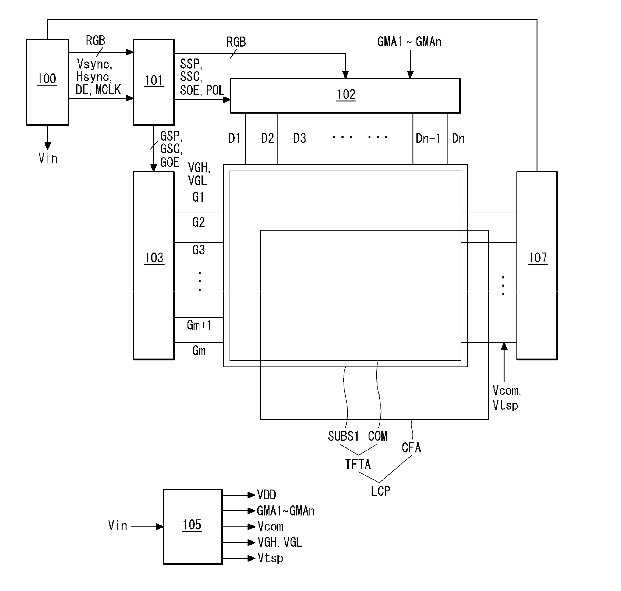
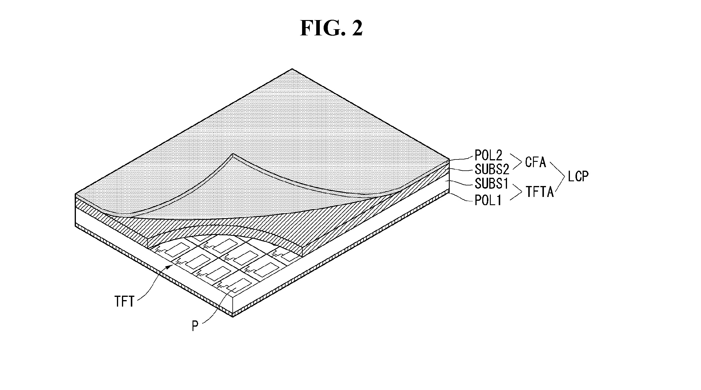
[0040]A touch sensor integrated display device on according to an embodiment of the present invention will be described in detail with reference to FIGS. 1 to 4. FIG. 1 is a view schematically illustrating a touch sensor integrated display device according to an embodiment of the present invention, FIG. 2 is a perspective view schematically illustrating a display panel of the display device illustrated in FIG. 1, FIG. 3 is a view schematically illustrating a relationship among a common electrode (touch electrodes), pixel electrodes, and circuit wiring patterns in a touch sensor integrated display device according to an embodiment of the present invention, and FIG. 4 is a view schematically illustrating an example of an arrangement relationship between a common electrode (touch electrodes) and pixel electrodes in a touch sensor integrated display device according to the present invention.

[0041]Hereinafter, a touch sensor integrated liquid crystal display device according to an embodi...

second embodiment

[0062]FIG. 8A is an enlarged plan view illustrating part of the touch sensor integrated display device according to the present invention, and FIG. 8B is a cross sectional view taken along a line III-III′ and a line IV-IV′ illustrated in FIG. 8A. As shown in FIGS. 8A and 8B, portions corresponding to the pixel electrodes P11 and P12 among the touch electrodes C11 of the common electrode COM of FIG. 3 are illustrated as examples, wherein the signal lines are connected to the touch electrodes in the direction of columns.

[0063]With reference to FIGS. 8A and 8B, the touch sensor integrated display device according to the second embodiment of the present invention includes a gate line G1 formed on the first substrate SUBS1 and a gate electrode G extending from the gate line G1.

[0064]The touch sensor integrated display device includes a gate insulating film G1 formed on the substrate SUBS1 on which the gate line G1 having the gate electrode G is formed, and a semiconductor pattern A which...

third embodiment

[0071]FIG. 10A is an enlarged plan view illustrating part of the touch sensor integrated display device according to the present invention and FIG. 10B is a cross sectional view taken along a line V-V′ and a line VI-VI′ illustrated in FIG. 10A. As shown in FIGS. 10A and 10B, portions corresponding to the pixel electrodes P11 and P12 among the touch electrodes C11 of the common electrode COM of FIG. 3 are illustrated as examples, wherein the signal lines are connected to the touch electrodes in the direction of column.

[0072]With reference to FIGS. 10A and 10B, the touch sensor integrated display device according to the third embodiment of the present invention includes a gate line G1 formed on the first substrate SUBS1, and a gate electrode G extending from the gate line G1.

[0073]The touch sensor integrated display device includes a gate insulating film G1 formed on the substrate SUBS1 on which the gate line G1 having the gate electrode G is formed, and a semiconductor pattern A whic...


PUM


Abstract

A touch sensor integrated display device is provided comprising gate lines and data lines formed on a substrate to be intersected with each other, a plurality of pixel electrodes formed at intersections between the gate lines and the data lines, and a common electrode formed to overlap the plurality of pixel electrodes through an insulating film disposed between the common electrode and the plurality of pixel electrodes, wherein the common electrode includes at least two touch electrodes, each of which is connected to at least one of signal lines arranged in one of a first direction and a second direction crossing the first direction.

Description

[0001]This application claims the benefit of Korean Patent Application Nos. 10-2011-0017181 filed on Feb. 25, 2011 and 10-2011-0077644 filed on Aug. 4, 2011, which are herein incorporated by reference.BACKGROUND[0002]1. Field[0003]This document relates to a display device, and more specifically to a touch sensor integrated display device.[0004]2. Related Art[0005]A touch sensor is a kind of input unit which is mounted on a video display device, such as a liquid crystal display (LCD), a field emission display (FED), a plasma display panel (PDP), an electroluminescence device (ELD), electrophoresis display (EPD), and so forth. While an image is displayed by the video display device, a user may contact, by pressing or touching, a touch panel on the video display device to input predetermined optional information through the touch sensor mounted in the video display device.[0006]Touch sensors used for display devices as described above may be largely divided into an add-on type, an on-c...

Claims


Application Information

Patent Timeline
Patent Type & Authority Applications(United States)
IPC IPC(8): G06F3/041
CPCG06F3/0412G06F3/044G02F2001/134372G02F1/13338G06F2203/04103G09G3/3648G09G2354/00G06F3/0446G02F1/134372G02F1/136286
Inventor KIM, CHEOLSELEE, BUYEOLLEE, SUNJUNGHWANG, SANGSOOWOO, YOONHWANHAN, MANHYEOP
Owner LG DISPLAY CO LTD
Why Eureka
Try Eureka