Use of high-K dielectric material in modified ONO structure for semiconductor devices

a technology of dielectric material and semiconductor device, which is applied in the direction of semiconductor devices, capacitors, electrical devices, etc., can solve the problems of reducing the charge trapping ability of the nitride layer, and limiting the scaling down of the total physical thickness of the ono layer. , to achieve the effect of reducing the equivalent oxide thickness of the ono, sacrificing the charge trapping ability of the modified on

Inactive Publication Date: 2003-11-04
MONTEREY RES LLC
View PDF15 Cites 268 Cited by
  • Summary
  • Abstract
  • Description
  • Claims
  • Application Information

AI Technical Summary

Benefits of technology

Thus, in the present invention, by use of a mid-K or a high-K dielectric material instead of silicon dioxide for the top oxide layer, a modified ONO structure may be fabricated having reduced dimensions without creation of interface states coming from contamination which could provide charge leakage paths within the modified ONO structure and without sacrificing the charge trapping ability of the modified ONO structure in the two-bit EEPROM device. The present invention provides advantages such as (1) reduction of equivalent oxide thickness of ONO in next generation devices; (2) high-K film devices are expected to have improved data retention and reliability; and (3) the high-K dielectric material layer replacing one of both silicon dioxide layers allows fabrication of an ONO layer which is physically thicker, resu

Problems solved by technology

However, as the ONO layer is made physically thinner, leakage current through the ONO layer may increase, and the charge trapping ability of the nitride layer may be reduced, which limits the scaling down of the total physical thickness of the ONO layer.
However, as the ONO layer is made physically thinner, leakage current through the ON

Method used


Image

  • Use of high-K dielectric material in modified ONO structure for semiconductor devices
  • Use of high-K dielectric material in modified ONO structure for semiconductor devices
  • Use of high-K dielectric material in modified ONO structure for semiconductor devices

Examples


Embodiment Construction

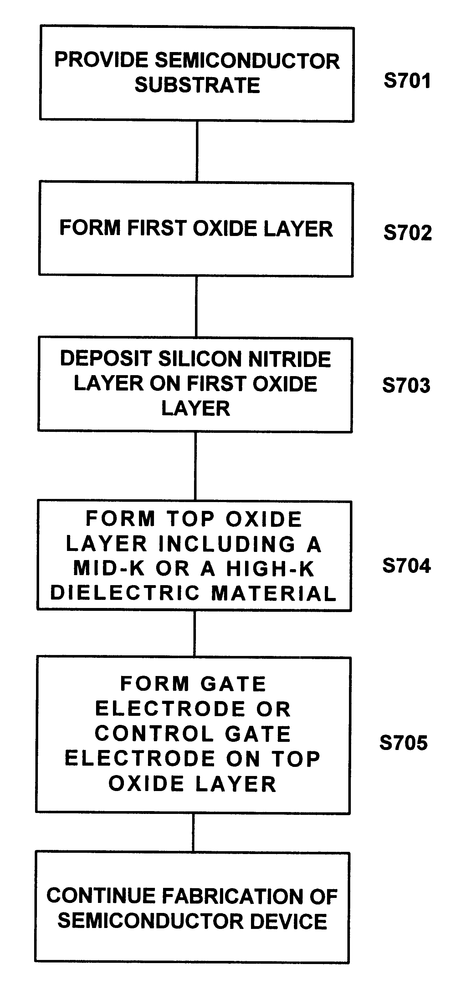
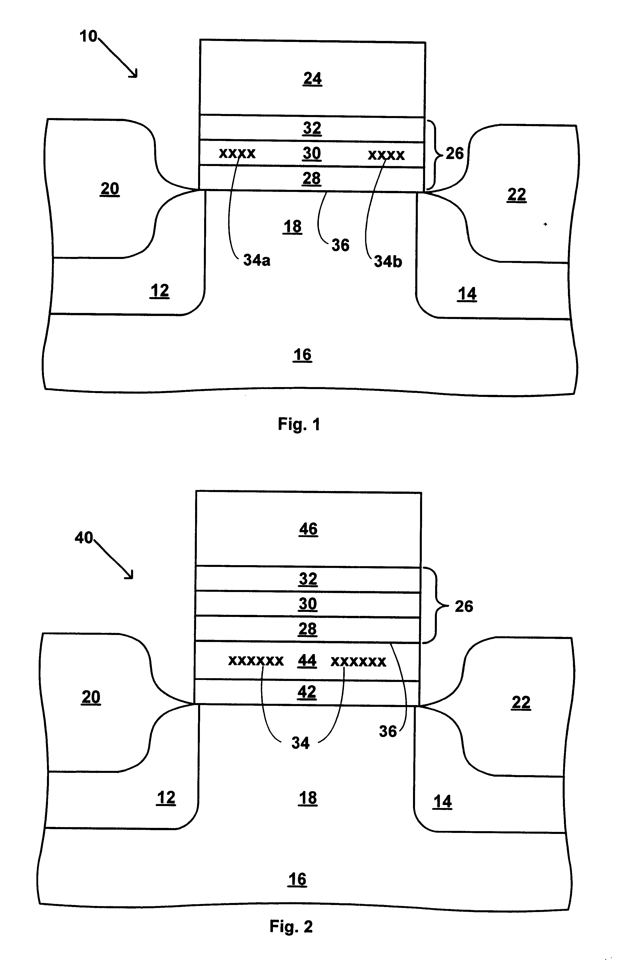
Referring first to FIG. 1, there is schematically shown in cross-section a transistor 10 suitable for use in a two-bit EEPROM device, such as the MIRRORBIT.TM. device. The transistor 10 includes source / drain regions 12 and 14 located in a semiconductor substrate 16 and separated by a channel region 18. First and second bit line oxide regions 20 and 22 overlie source / drain regions 12 and 14, respectively. A gate electrode 24 overlies the channel region 18 and is separated therefrom by a modified ONO structure 26. The gate electrode 24 and the modified ONO structure 26 form a stacked-gate structure. The modified ONO structure 26 includes a first or tunnel dielectric material layer 28, a silicon nitride layer 30 and a top dielectric material layer 32, in that order, as shown in FIG. 1. At least one of the top dielectric material layer 32 and the bottom dielectric material layer 28 comprises a mid-K or high-K dielectric material, which replaces the conventional silicon dioxide material ...


PUM


Abstract

A process for fabrication of a semiconductor device including a modified ONO structure, comprising forming the modified ONO structure by providing a semiconductor substrate; forming a first dielectric material layer on the semiconductor substrate; depositing a silicon nitride layer on the first dielectric material layer; and forming a top dielectric material layer, wherein at least one of the bottom dielectric material layer and the top dielectric material layer comprise a mid-K or a high-K dielectric material. The semiconductor device may be, e.g., a SONOS two-bit EEPROM device or a floating gate flash device including the modified ONO structure.

Description

The present invention relates to a process for preparation of a semiconductor device including forming a modified ONO structure. The modified ONO structure comprises a high-K dielectric material.Non-volatile memory devices are currently in widespread use in electronic components that require the retention of information when electrical power is terminated. Non-volatile memory devices include read-only-memory (ROM), programmable-read-only memory (PROM), erasable-programmable-read-only memory (EPROM), and electrically-erasable-programmable-read-only-memory (EEPROM) devices. EEPROM devices differ from other non-volatile memory devices in that they can be electrically programmed and erased. Flash EEPROM devices are similar to EEPROM devices in that memory cells can be programmed and erased electrically. However, flash EEPROM devices enable the erasing of all memory cells in the device using a single electrical current pulse.Product development efforts in EEPROM device technology have fo...

Claims


Application Information

Patent Timeline
IPC IPC(8): H01L21/28H01L29/51H01L21/02H01L21/316H01L21/314H01L29/40H01L21/318
CPCH01L21/28185H01L21/28273H01L21/28282H01L21/3143H01L21/3144H01L21/31604H01L21/31691H01L29/513H01L29/516H01L29/517H01L29/518H01L21/28194Y10S438/954H01L21/28202H01L21/28211H01L21/3185H01L28/56H01L29/40114H01L29/40117H01L21/02192H01L21/02271H01L21/02142H01L21/02175H01L21/02178H01L21/02186H01L21/02211H01L21/02189H01L21/02194H01L21/02205H01L21/02181H01L21/0217H01L21/02197
Inventor HALLIYAL, ARVINDRAMSBEY, MARK T.ZHANG, WEIRANDOLPH, MARK W.CHEUNG, FRED T. K.
Owner MONTEREY RES LLC
Why Eureka
Try Eureka