Bridge Resistance Random Access Memory Device and Method With A Singular Contact Structure
a memory device and resistance technology, applied in semiconductor devices, semiconductor/solid-state device details, electrical devices, etc., can solve the problems of large space occupation of contacts in resistance memory devices, and the manufacturing of such devices with very small dimensions, so as to reduce the overall dimension of memory cells
- Summary
- Abstract
- Description
- Claims
- Application Information
AI Technical Summary
Benefits of technology
Problems solved by technology
Method used
Image
Examples
first embodiment
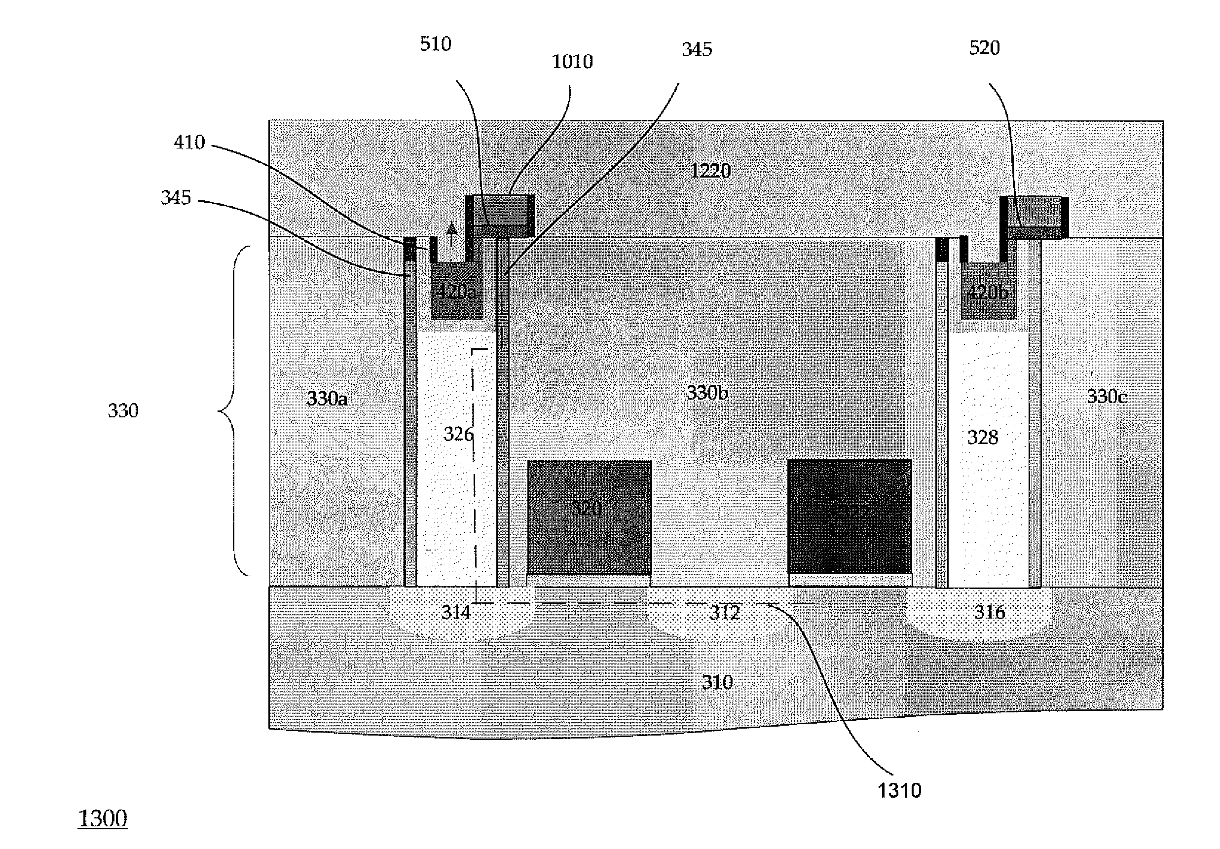
[0034]FIG. 3 illustrates a cross-sectional view of a process diagram showing a first step in the manufacturing of a bistable resistive random access memory 300 with the formation of a transistor structure in accordance with the The bistable resistive random access memory 300 is formed on a semiconductor substrate 310. Access transistors are formed by an n-type terminal 312 acting as a common source region and n-type terminals 314 and 316 acting as drain regions in the p-type substrate 310. Polysilicon word (gate) lines 320, 322 form the gates of the access transistors. An inter-layer dielectric 330 includes dielectric fills 330a, 330b and 330c where the dielectric fill 330b is formed over the polysilicon word lines 320, 322. Suitable materials for implementing the inter-layer dielectric 330 include BPSG oxide and PETEOS oxide. The inter-layer dielectric 330 is patterned and conductive structures, including a common source line (not shown) and contact structures 326 and 328, are for...
third embodiment
[0048]FIG. 10 is a process diagram 1000 illustrating a cross-sectional view of the bridge resistance random access memory with the deposition of a hard mask on a resistance memory material bridge. A top surface of the second electrode 420 is polished to remove excess materials that are outside the contact structures 326, 328, which results in a second electrode 420a in the first contact structure 326 and a second electrode 420b in the second contact structure 328. Embodiments of the process for polishing include a chemical mechanical polishing process, followed by brush clean and liquid and / or gas clean procedures, as known in the art. Alternatively, the chemical mechanical polishing may be conducted to an over-polish degree in order to enable the liner dielectric 410 that may protrude beyond the contact structure 326 to also be removed. The second electrode 420a is separated from the first electrode 345 by the thin liner dielectric 410. Top surfaces of the first electrode 345, the ...
PUM
 Abstract
Description
Claims
Application Information


