Light emitting diode package with improved optical lens structure

a technology of light-emitting diodes and optical lenses, applied in the field of semiconductor packages, can solve the problems of insufficient bonding strength, unsatisfactory reliability, and thin lens configuration

Active Publication Date: 2014-09-16
ADVANCED OPTOELECTRONICS TECH
View PDF6 Cites 25 Cited by
  • Summary
  • Abstract
  • Description
  • Claims
  • Application Information

AI Technical Summary

Benefits of technology

[0005]The LED package generally includes a substrate, an LED die arranged on the substrate, and a lens adhered on the substrate by glue to adjust light from the LED die. However, the lens is usually configured very thin to satisfy compact requirement of the LED package. Accordingly, a contact area of the lens and the substrate is quite small, thereby leading to inadequate bond strength and unsatisfied reliability thereof.

Problems solved by technology

However, the lens is usually configured very thin to satisfy compact requirement of the LED package.
Accordingly, a contact area of the lens and the substrate is quite small, thereby leading to inadequate bond strength and unsatisfied reliability thereof.

Method used


Image

  • Light emitting diode package with improved optical lens structure
  • Light emitting diode package with improved optical lens structure
  • Light emitting diode package with improved optical lens structure

Examples


Embodiment Construction

[0011]Reference will now be made to the drawings to describe an exemplary embodiment of the present LED package.

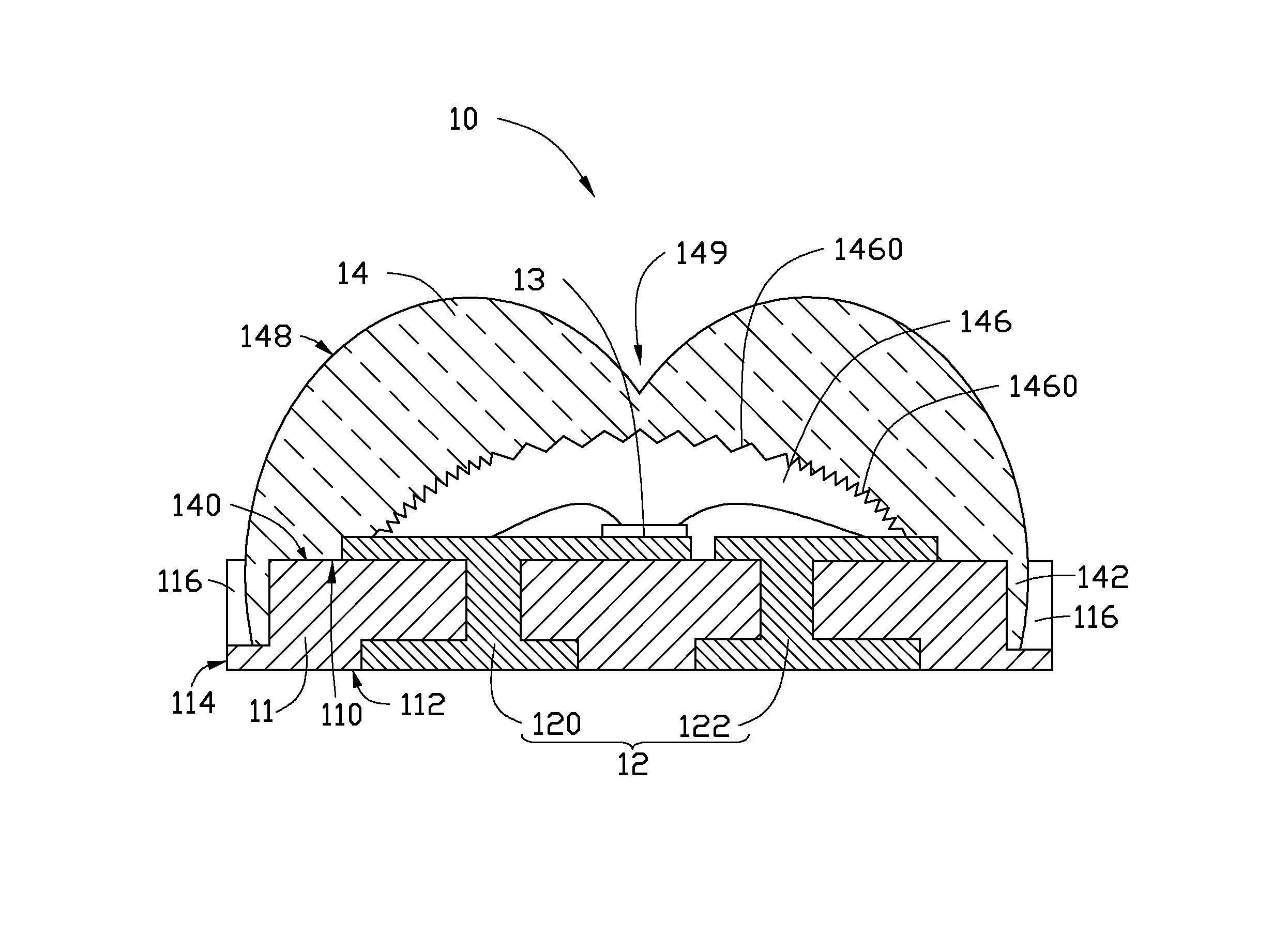
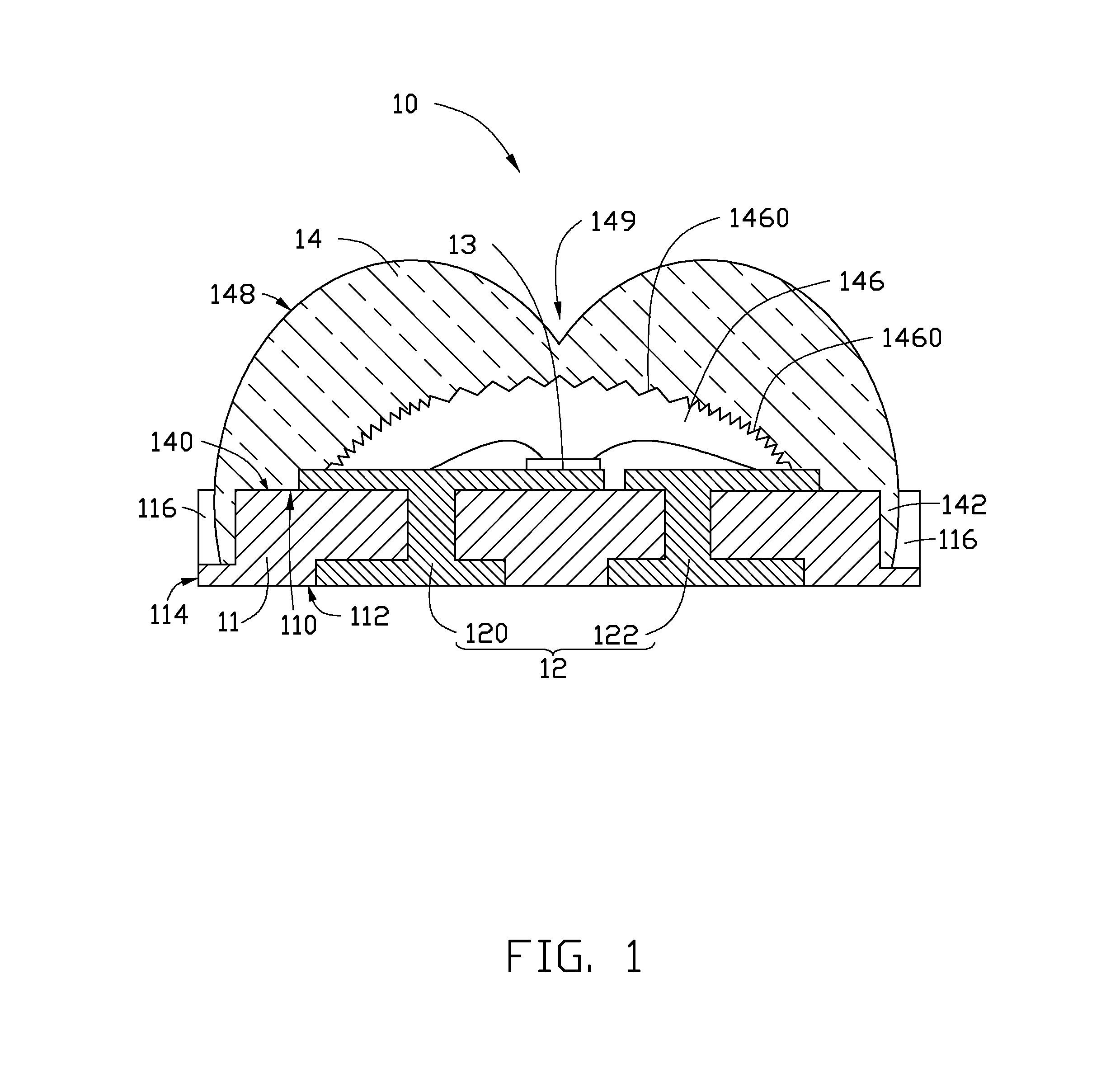
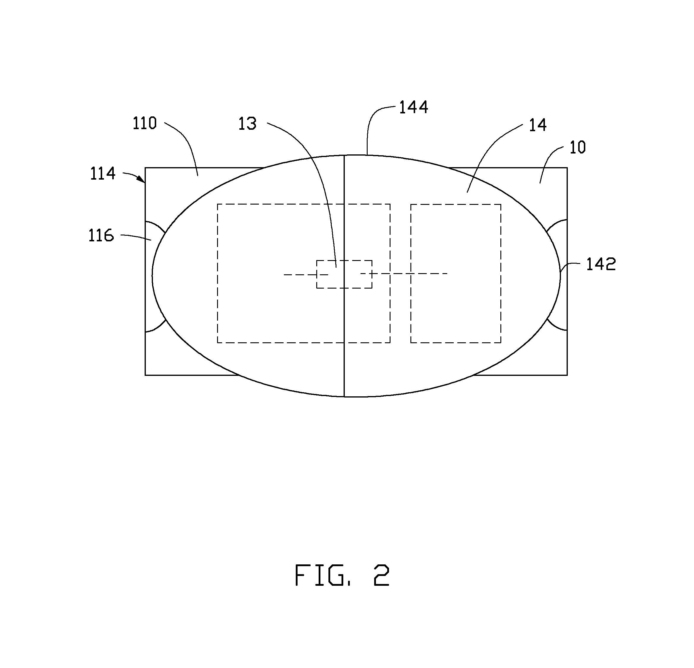
[0012]Referring to FIG. 1 and FIG. 2, an LED package 10, in accordance with an exemplary embodiment of the present disclosure, includes a substrate 11, two electrodes 12, an LED die 13 and a lens 14.

[0013]The substrate 11 can be made of a circuit board such as a metal-cored printed circuit board (MCPCB). The substrate 11 includes a top surface 110, a bottom surface 112, and four side surfaces 114 each interconnecting the top surface 110 with the bottom surface 112. Two notches 116 are configured depressed downward from opposite lateral peripheral portions of the top surface 110. In this embodiment, the top surface 110 has a rectangular shape, and the two notches 116 are configured at two opposite short sides of the rectangle.

[0014]The two electrodes 12 each penetrate through the substrate 11, and each electrode 12 is exposed at both the top surface 110 and the bottom surfa...


PUM


Abstract

An LED package includes a substrate, two electrodes, an LED die and a lens. The substrate includes a top surface, a bottom surface, a plurality of side surfaces interconnecting the top surface with the bottom surface, and two opposite notches depressed downward from lateral peripheral portions of the top surface. The two electrodes penetrate through the substrate, and each of the two electrodes is exposed at both the top surface and the bottom surface of the substrate. The LED die is arranged on the substrate and electrically connected to the two electrodes. The lens is arranged on the substrate and covers the LED die. The lens includes a contacting surface adjoining the top surface of the substrate, and two protrusions extending from lateral peripheral portions of the contacting surface and respectively embedded in the two notches.

Description

BACKGROUND[0001]1. Technical Field[0002]The present disclosure generally relates to semiconductor packages, and particularly to a light emitting diode (LED) package which has an improved optical lens structure.[0003]2. Description of Related Art[0004]In recent years, due to excellent light quality and high luminous efficiency, light emitting diodes (LEDs) have increasingly been used as substitutes for incandescent bulbs, compact fluorescent lamps and fluorescent tubes as light sources of illumination devices.[0005]The LED package generally includes a substrate, an LED die arranged on the substrate, and a lens adhered on the substrate by glue to adjust light from the LED die. However, the lens is usually configured very thin to satisfy compact requirement of the LED package. Accordingly, a contact area of the lens and the substrate is quite small, thereby leading to inadequate bond strength and unsatisfied reliability thereof.[0006]Therefore, it is necessary to provide an LED package...

Claims


Application Information

Patent Timeline
Patent Type & Authority Patents(United States)
IPC IPC(8): H01L33/00H01L31/0203
CPCH01L33/58H01L33/486H01L2224/48091H01L2924/00014
Inventor HSIEH, YU-LUN
Owner ADVANCED OPTOELECTRONICS TECH
Why Eureka
Try Eureka