Large-area bulk gallium nitride wafer and method of manufacture

a gallium nitride and large-area bulk technology, applied in the direction of crystal growth process, polycrystalline material growth, synthetic resin layered products, etc., can solve the problems of high defect density of epitaxial films, low defect density, and high volume production of devices, so as to achieve low defect density and cost-effective

Active Publication Date: 2011-11-01
SLT TECH
View PDF2 Cites 56 Cited by
  • Summary
  • Abstract
  • Description
  • Claims
  • Application Information

AI Technical Summary

Benefits of technology

[0016]One or more benefits may be achieved using one or more of the specific embodiments. As an example, the present device and method provides a substantially flat and large area seed crystal having high quality and low defect density, suitable for ammonothermal growth or growth by another bulk growth process, including but not limited to solution growth, high pressure solution growth, liquid phase epitaxy, physical vapor transport, and melt growth. In a specific embodiment, the present method and device can be made using conventional techniques and is cost effective. In a specific embodiment, the present wafer provides a cost-effective route to high-quality large-area bulk GaN substrates which are currently of very limited availability. In a specific embodiment, the present wafer can be used for ammonothermal growth of a volume of gallium nitride which can be subsequently cut into wafers of suitable size and quality for use as substrates. In a preferred embodiment, the present method and device provide for high quality, low-defect, large-area bulk gallium nitride substrates to enable performance enhancements in gallium nitride-based electronic and optoelectronic devices which have a variety of growing commercial applications. The present invention provides such a high-quality large-area gallium nitride wafer in one or more embodiments. Depending upon the embodiment, one or more of these benefits can be achieved. These and other benefits are further described throughout the present specification and more particularly below.

Problems solved by technology

Although some of these products are available in the commercial market today, lack of a suitable GaN substrate on which to grow these materials remains a limitation to both performance and providing low cost, volume production of devices.
Heteroepitaxial approaches to growth of (Al,In)GaN containing compounds result in epitaxial films with high defect densities (commonly 1010 cm-2 or higher) due to the large lattice mismatch, chemical dissimilarity and thermal expansion coefficient difference between the nitride materials and substrate.
The presence of defects is well-known to be detrimental to device performance.
Additionally, heteroepitaxy of gallium nitride and related materials on foreign substrates can result in incorporation of impurities into the gallium nitride material.
Ammonothermal growth has provided high quality crystalline material, however, drawbacks exist.
As an example, ammonothermal growth techniques currently lead to small sized crystals, which are often not useful for commercial applications.
Additionally, a significant limitation is that defects in the seed material used for ammonothermal growth are known to replicate on any grown crystal structures.
These and other limitations often exist with ammonothermal techniques.

Method used


Image

  • Large-area bulk gallium nitride wafer and method of manufacture
  • Large-area bulk gallium nitride wafer and method of manufacture
  • Large-area bulk gallium nitride wafer and method of manufacture

Examples


Embodiment Construction

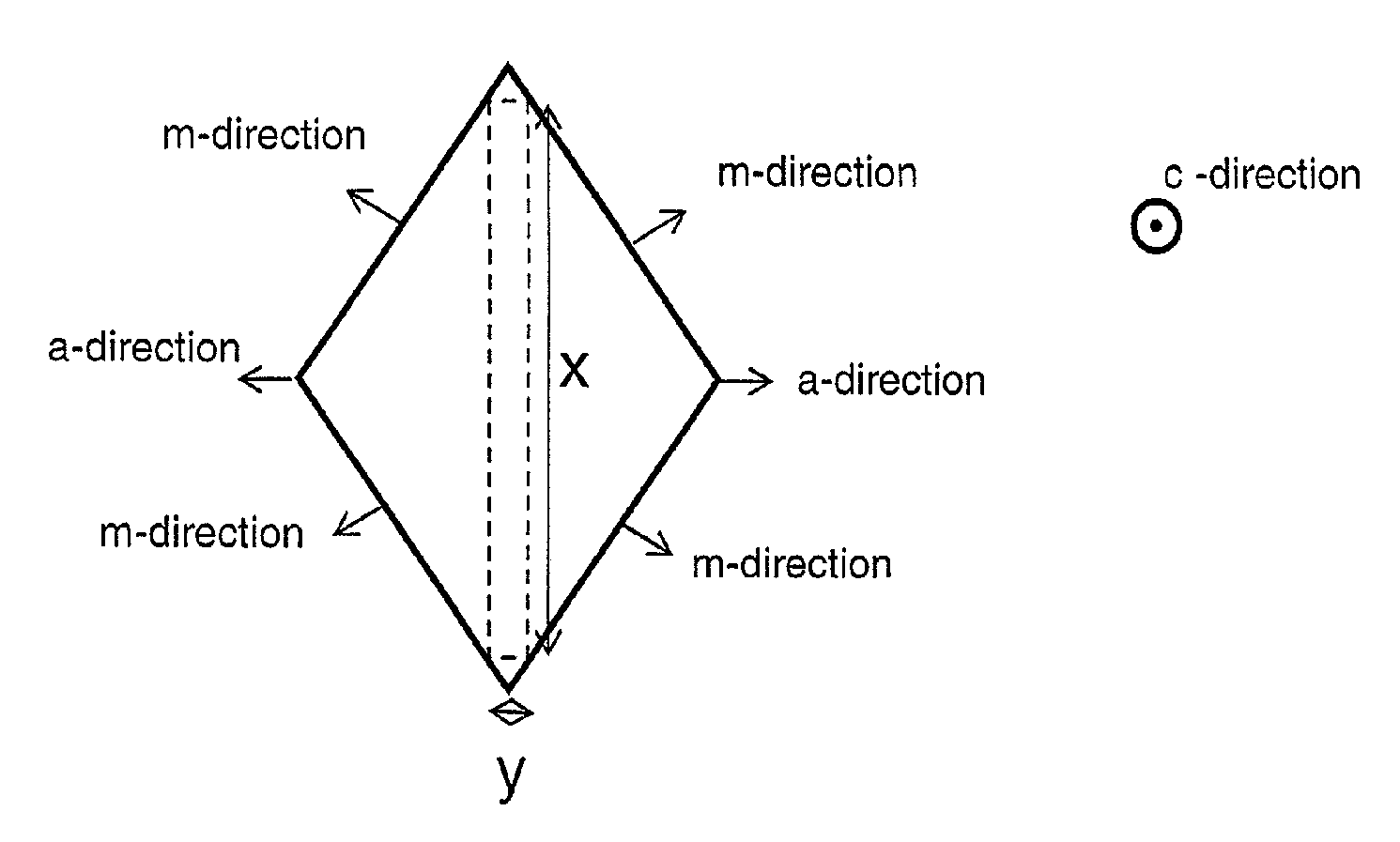
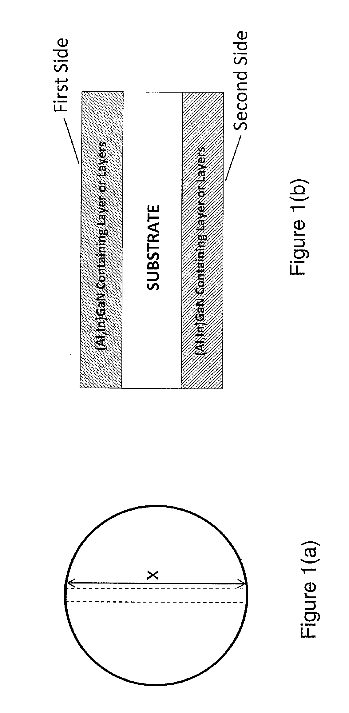
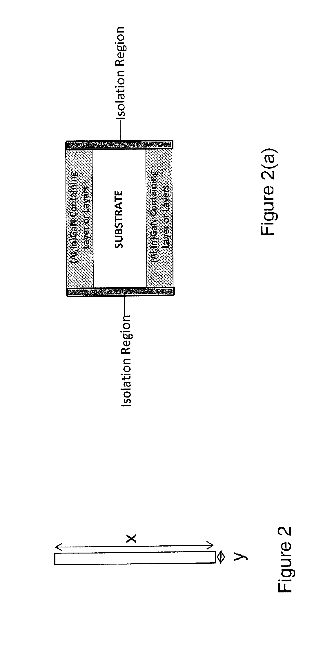
[0040]According to the present invention, techniques for manufacture of crystalline materials are provided. More particularly, the present invention provides a large-area bulk gallium nitride wafer and method of manufacture. In a specific embodiment, the bulk gallium nitride wafer can be used in an ammonothermal growth process or the like. In a specific embodiment, the wafer can be further used to produce large-volume bulk gallium nitride crystals which can be cut into wafers for use as substrates. Merely by way of example, the present wafer can be used in applications such as such as light emitting diodes, integrated circuits, MEMS, medical devices, combination of these, among others.

[0041]According to specific embodiment of the present invention, techniques are provided for manufacture of a bulk gallium nitride wafer which is large-area, substantially free of bowing, substantially defect-free, and free of foreign substrate materials. Such a wafer can be used, for example, as a see...


PUM

PropertyMeasurementUnit
lengthaaaaaaaaaa
diameteraaaaaaaaaa
diameteraaaaaaaaaa

Abstract

The present invention includes a high-quality, large-area bulk GaN seed crystal for ammonothermal GaN growth and method for fabricating. The seed crystal is of ultra-low defect density, has flat surfaces free of bowing, and is free of foreign substrate material. The seed crystal is useful for producing large-volume, high-quality bulk GaN crystals by ammonothermal growth methods for eventual wafering into large-area GaN substrates for device fabrication.

Description

CROSS-REFERENCES TO RELATED APPLICATIONS[0001]This application claims priority to U.S. Provisional Application No. 61 / 148,361 filed Jan. 29, 2009 and U.S. Provisional Application No. 61 / 181,513 filed May 27, 2009, commonly assigned, both of which are incorporated by reference in their entirety herein.[0002]This application is related to U.S. application Ser. No. 12 / 556,558, filed Sep. 9, 2009, commonly assigned, of which is incorporated by reference in its entirety herein.[0003]The seed structure described in Poblenz, Christiane, et al., U.S. Provisional Application No. 61 / 096,304 filed Sep. 9, 2008, commonly assigned, and hereby incorporated by reference herein along with U.S. Provisional Application No. 61 / 178,460 filed May 14, 2009.BACKGROUND OF THE INVENTION[0004]The present invention relates generally to crystalline materials. More particularly, the present invention provides an ultra-low defect density, large-area bulk gallium nitride wafer which is free of bowing. The resulti...

Claims


Application Information

Patent Timeline
Patent Type & Authority Patents(United States)
IPC IPC(8): C30B21/04
CPCC30B23/025C30B25/18C30B29/403C30B29/406
Inventor POBLENZ, CHRISTIANESCHMIDT, MATHEW C.KAMBER, DERRICK S.
Owner SLT TECH
Why Eureka
Try Eureka