Non-polar iii-v nitride material and production method

a nitride material and non-polar technology, applied in the direction of polycrystalline material growth, polycrystalline material growth, chemically reactive gas growth, etc., can solve the problems of redshift emission, disruption of current trend of polar materials, and increase of radiative recombination time at the expense of quantum efficiency, etc., to achieve low defect density and low stress

Active Publication Date: 2009-03-26
QUANTUM NIL LTD +1
View PDF11 Cites 48 Cited by
  • Summary
  • Abstract
  • Description
  • Claims
  • Application Information

AI Technical Summary

Benefits of technology

[0009]In one embodiment, the current invention is directed to method of producing non-polar III nitride materials having both low defect density and low stress.

Problems solved by technology

Consequently, when using these conventional materials the radiative recombination time increases at the expense of quantum efficiency and a red-shift of the emission occurs.
However, the use of non-polar III nitride materials for semiconductor devices such as high current density drive light-emitting diodes (LEDs) and laser diodes (LDs) may disrupt the current trend for polar materials.
Unfortunately, this technology suffers from a low growth rate and is limited to small diameter substrates, making these materials very expensive and uneconomic for commercial manufacturing.
However, the HVPE technique still has the same inherent problems as other growth techniques due to its growth on foreign substrates.
However, growth processes using these techniques are tedious, time consuming and expensive.
Moreover, the GaN produced using such techniques still has the major disadvantage of being subject to bending and undesired residual strain.

Method used


Image

  • Non-polar iii-v nitride material and production method
  • Non-polar iii-v nitride material and production method
  • Non-polar iii-v nitride material and production method

Examples


example 1

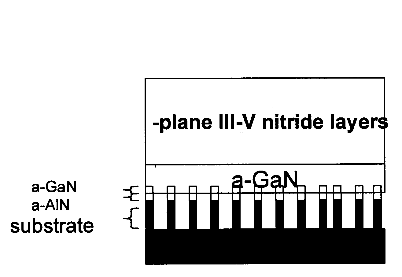
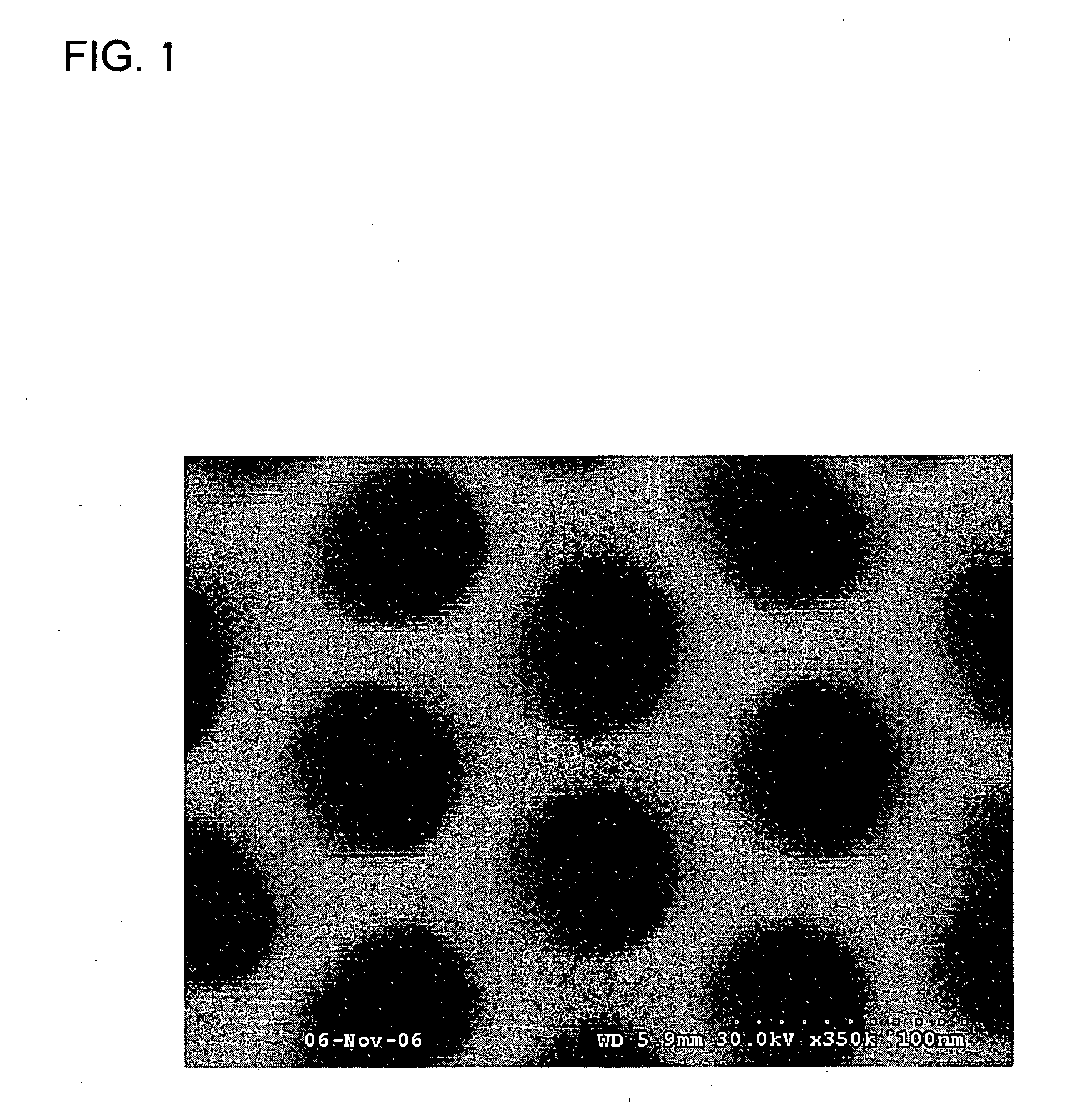
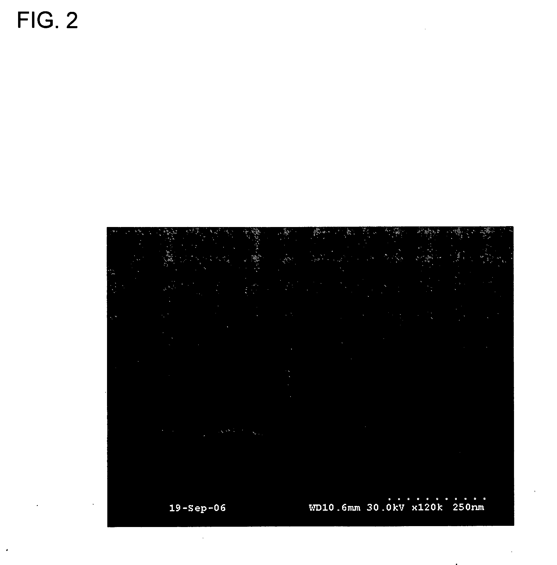
[0068]A γ-plane-oriented sapphire substrate of about 2 inches (5.08 cm) in diameter with MOCVD-deposited a-plane AlN (20 nm) and GaN of about 0.6 μm is loaded onto the substrate holder of a HVPE vertical reactor. Before loading, the a-plane GaN template is degreased in KOH for a few seconds, rinsed in deionized water, etched in a H2SO4 / H3PO4=3:1 solution at 80° C. for a few minutes, then rinsed in deionized water. It is then necessary to create a mask onto the template. Firstly, a thin dielectric layer of SiO2 or Si3N4 of ˜200 nm is deposited by PECVD onto the GaN template. Then a thin Al metal of about 60-200 nm is deposited by e-beam evaporation or sputtering onto the dielectric layer. A two step anodization process is used. A first anodization is conducted under 0.3 M oxalic acid solution at 5° C. with current ˜100 mA and 20 V for about 6 hours to form a layer of oxide (alumina) on top of the aluminium layer. The surface texture of the aluminium is changed by the anodization proc...

example 2

[0075]Here, the initial MOCVD epitaxial lateral overgrowth process described in Example 1 is replaced by a combined pulsed and normal MOCVD growth method. In this method, the flow sequence of reagent gases is on (NH3 and TMG on) and off (TMG on and NH3 off) in turn for the enhanced lateral growth mode. The time for the on and off period is set to be around 20-60 seconds and 10-15 seconds respectively. The a-plane n-GaN growth step is continued until a continuous a-plane n-GaN epitaxial layer is produced. Then a full non-polar LED device structure is grown on top of the a-plane GaN. Then a Ni (10 nm) / Au(10 nm) contact is deposited, annealed in O2 at 550° C. for 1 minute. Ti / Al / Ti / Au with Al as the reflector is then deposited on top of the Ni / Au contact. The non-polar device is then solder bonded to a submount for good thermal management. The submount may comprise SiC, CVD diamond, AlN, metals, alloys or Silicon. The substrate / template is then removed as before.

example 3

[0076]In this Example, the thick non-polar m-plane n-GaN is grown on the nano-pores and nano-networks template, wherein the nano-network surrounding the nano-pores comprises non-polar m-plane GaN, AlN, and (100) LiAlO2. (100) LiAlO2 is weakened by further wet etching using diluted HCl. The thick m-plane n-GaN is separated from the substrate through the mechanical cracking of the weakened (100) LiAlO2 nano-networks.


PUM

PropertyMeasurementUnit
thicknessaaaaaaaaaa
thicknessaaaaaaaaaa
total thicknessaaaaaaaaaa

Abstract

A method for growing flat, low defect density, and strain-free thick non-polar III-V nitride materials and devices on any suitable foreign substrates using a fabricated nano-pores and nano-network compliant layer with an HVPE, MOCVD, and integrated HVPE/MOCVD growth process in a manner that minimum growth will occur in the nano-pores is provided. The method produces nano-networks made of the non-polar III-V nitride material and the substrate used to grow it where the network is continuous along the surface of the template, and where the nano-pores can be of any shape.

Description

FIELD OF THE INVENTION[0001]The present invention is directed to methods of producing non-polar III nitride materials having both low defects density and low stress, and more particularly to a method utilizing a fabricated nano-pores and nano-network compliant layer with an HVPE, MOCVD, and integrated HVPE / MOCVD growth process.BACKGROUND OF THE INVENTION[0002]Wide band-gap III-V nitride materials are recognized to be among the most attractive compound semiconductors for use in a variety of devices. They are suitable for optoelectronic and microelectronic devices that operate in a wide spectral range, from visible to ultraviolet, and in the high temperature / high power applications area. The main advantage of nitride semiconductors in comparison with other wide-band-gap semiconductors is their low propensity to degrade at high temperature and high power when used for optical and microelectronic devices.[0003]Current commercial nitride semiconductor products are typically based on c-ax...

Claims


Application Information

Patent Timeline
Patent Type & Authority Applications(United States)
IPC IPC(8): H01L29/20H01L21/36
CPCB82Y30/00C30B25/02C30B29/403H01L21/0237H01L21/0265H01L21/02513H01L21/0254H01L21/0262H01L21/02639H01L21/02458
Inventor WANG, WANG NANG
Owner QUANTUM NIL LTD
Why Eureka
Try Eureka