

Low-temperature bonding method for semiconductor without oxide layer
A low-temperature bonding, semiconductor technology, used in semiconductor/solid-state device manufacturing, electrical components, circuits, etc., can solve problems such as photoelectric performance degradation, limiting carrier transport, and limiting the application of Ge/Si heterogeneous materials. And the effect of cost and low cost
- Summary
- Abstract
- Description
- Claims
- Application Information
AI Technical Summary
Problems solved by technology
Method used
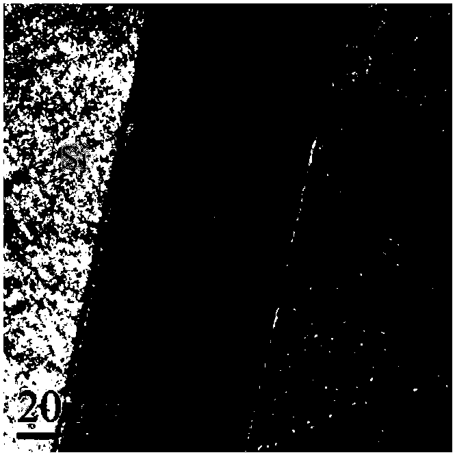
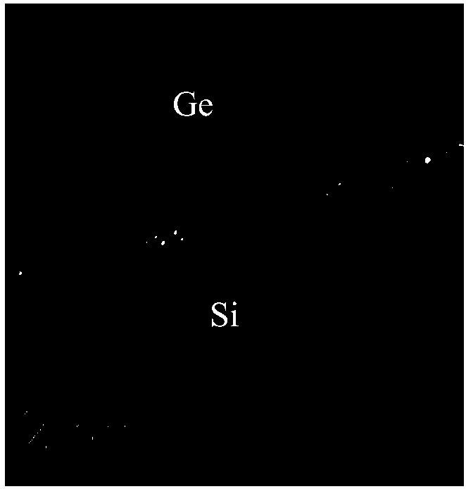
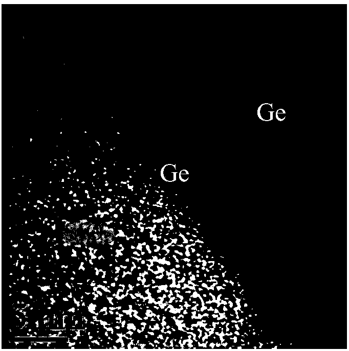
Image

Examples
Embodiment 1
[0042] The equipment used is a TRP-450 composite film sputtering deposition system, and two DC targets and one RF target are placed in the growth chamber. The target material used is a high-purity Ge circular target material of 5N (above 99.999%). The used Si substrate material is a (100) N-type single crystal Si wafer, polished on one side, and has a resistivity of 1-5Ω·cm.
[0043] 1. Treatment of Si substrate materials
[0044] 1) Select a Si substrate with a crystal orientation of (100), and ultrasonically clean it with acetone, ethanol, and deionized water for 10 minutes respectively to remove particles and organic matter attached to the surface of the substrate;
[0045] 2) The Si sheet after the organic ultrasonic cleaning was first washed with H 2 SO 4 :H 2 o 2 = 4:1 solution was boiled for 10 minutes, rinsed with deionized water for 15 times, and then HF:H 2 Soak in O=1:20 solution for 2mim, rinse with deionized water for 15 times;
[0046] 3) Then use NH 4 OH...
Embodiment 2
[0055] The equipment used is a TRP-450 composite film sputtering deposition system, and two DC targets and one RF target are placed in the growth chamber. The target material used is a high-purity Ge circular target material of 5N (above 99.999%). The Si substrate material used is an N-type single crystal Si wafer with a crystal orientation of (100), polished on one side, and the resistivity is 1-5 Ω cm, and the Ge substrate material used is a P-type single crystal with a crystal orientation of (100). Ge wafer, polished on one side, resistivity 0.05Ω·cm.
[0056] 1. Treatment of Si and Ge substrate materials
[0057] 1) Select Si and Ge substrates with a crystal orientation of (100), and use acetone, ethanol, and deionized water to ultrasonically clean them for 10 minutes, respectively, to remove particles and organic matter attached to the surface of the substrate;
[0058] 2) The Si sheet after the organic ultrasonic cleaning was first washed with H 2 SO 4 :H 2 o 2 = 4...
Embodiment 3
[0069]The equipment used is a TRP-450 composite film sputtering deposition system, and two DC targets and one RF target are placed in the growth chamber. The target material used is a high-purity Ge circular target material of 5N (above 99.999%). The Si substrate material used is an N-type single crystal Si sheet with a crystal orientation of (100), polished on one side, with a resistivity of 1-5Ω cm, and the top layer is thermally oxidized SiO 2 The thickness of the substrate is 200nm, and the Ge substrate material used is a P-type single crystal Ge sheet with crystal orientation (100), polished on one side, and the resistivity is 0.05Ω·cm.
[0070] 1. SiO2 2 / Processing of Si and Ge substrate materials
[0071] 1) Select SiO with a crystal orientation of (100) 2 / Si and Ge substrates were ultrasonically cleaned with acetone, ethanol, and deionized water for 10 minutes, respectively, to remove particles and organic matter attached to the surface of the substrate;
[0072...
PUM
| Property | Measurement | Unit |
|---|---|---|
| electrical resistivity | aaaaa | aaaaa |
| electrical resistivity | aaaaa | aaaaa |
| thickness | aaaaa | aaaaa |
Abstract
Description
Claims
Application Information