

Method of manufacturing bonding structure for multi-layer bonding stack and bonding structure
A technology of bonding structure and manufacturing method, which is applied in semiconductor/solid-state device manufacturing, semiconductor/solid-state device components, semiconductor devices, etc., can solve problems such as increased chip resistance, reduced bandwidth, and limited freedom of circuit design. Improve the effective use of area, reduce bandwidth reduction, and reduce the effect of large resistance
- Summary
- Abstract
- Description
- Claims
- Application Information
AI Technical Summary
Problems solved by technology
Method used
Image

Examples
Embodiment Construction
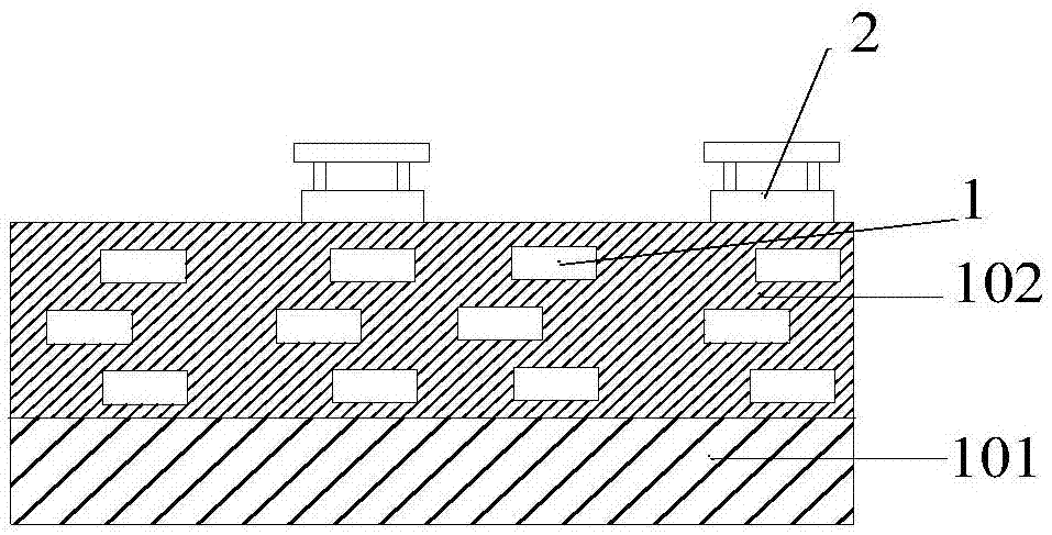
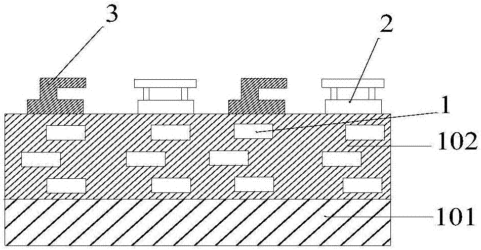
[0042] In the following description, for purposes of illustration rather than limitation, specific details such as specific system architectures, interfaces, and techniques are set forth in order to provide a thorough understanding of the present invention. It will be apparent, however, to one skilled in the art that the invention may be practiced in other embodiments without these specific details. In other instances, detailed descriptions of well-known systems, circuits, and methods are omitted so as not to obscure the description of the present invention with unnecessary detail.
[0043] An integrated circuit (integrated circuit) is a tiny electronic device or component. Using a certain process, the transistors, resistors, capacitors, inductors and other components required in a circuit are interconnected together, fabricated on a small or several small semiconductor wafers or dielectric substrates, and then packaged in a tube shell Inside, it becomes a microstructure with...
PUM
 Abstract
Description
Claims
Application Information