Semiconductor transistor preparation method and structure

A semiconductor and transistor technology is applied in the field of preparation method and structure of semiconductor transistors to achieve the effects of improving stability and reliability, reducing resistance-capacitance delay, and reducing parasitic capacitance

Pending Publication Date: 2018-05-25
CHANGXIN MEMORY TECH INC
View PDF7 Cites 3 Cited by
  • Summary
  • Abstract
  • Description
  • Claims
  • Application Information

AI Technical Summary

Problems solved by technology

[0005] In view of the above-mentioned shortcomings of the prior art, the purpose of the present invention is to provide a method and structure for the preparation of a semiconductor transistor, which is used to solve the problems between the gate and the plug conductive structure, as well as the plug conductive structure and the plug conductive structure in the prior art. The problem of large parasitic capacitance between, improve device stability and reliability

Method used


Image

  • Semiconductor transistor preparation method and structure
  • Semiconductor transistor preparation method and structure
  • Semiconductor transistor preparation method and structure

Examples


Embodiment 1

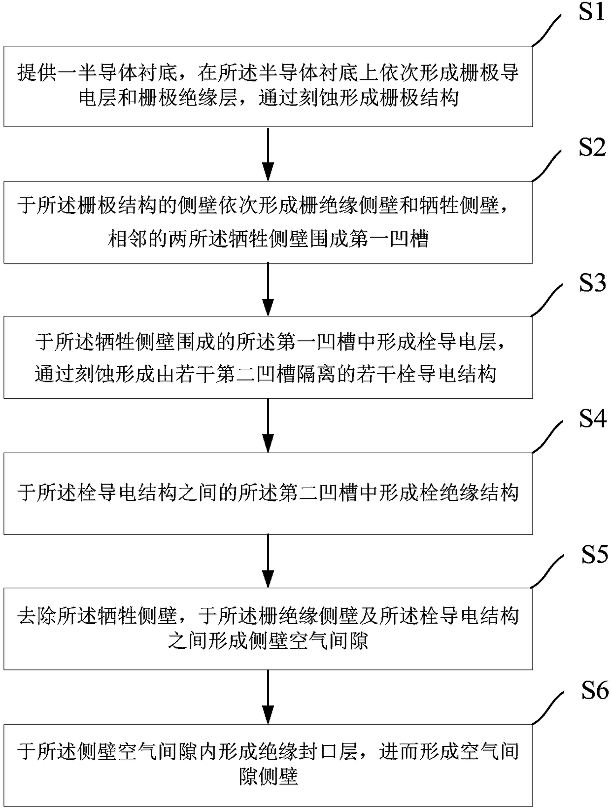
[0115] Such as Figure 2 to Figure 17 As shown, in order to effectively reduce the parasitic capacitance between the gate and the plug conductive structure, reduce the resistance-capacitance delay, increase the switching speed, and reduce the switching energy, this embodiment provides a method for preparing a semiconductor transistor structure. The semiconductor transistor structure The preparation method comprises the following steps at least:

[0116] Step S1 is executed to provide a semiconductor substrate 11 on which a gate conductive layer 121 and a gate insulating layer 122 are sequentially formed, and a gate structure is formed by etching.

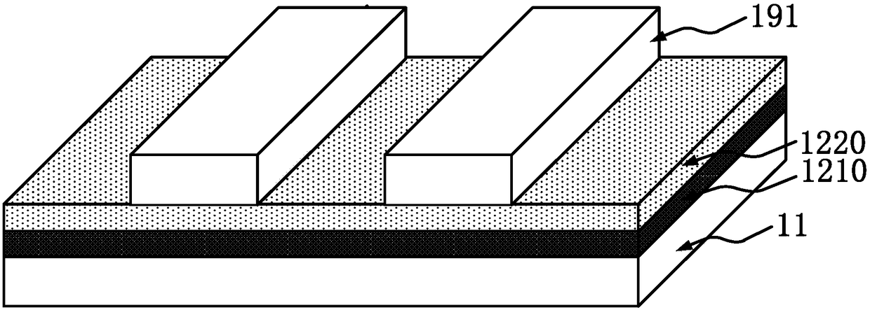
[0117] Specifically, such as image 3 As shown, in this embodiment, the semiconductor substrate 11 adopts a silicon substrate; an oxide layer (not shown in the figure) is oxidized on the silicon substrate as a dielectric layer of the gate structure, with a thickness of Between 1 nanometer and 10 nanometers; using physical vapor de...

Embodiment 2

[0153] Such as Figure 2 to Figure 13 with Figure 18 ~ Figure 22 As shown, this embodiment provides a method for preparing a semiconductor transistor structure, and the method for preparing a semiconductor transistor structure at least includes the following steps:

[0154] Step S1 is executed to provide a semiconductor substrate 11 on which a gate conductive layer 121 and a gate insulating layer 122 are sequentially formed, and a gate structure is formed by etching.

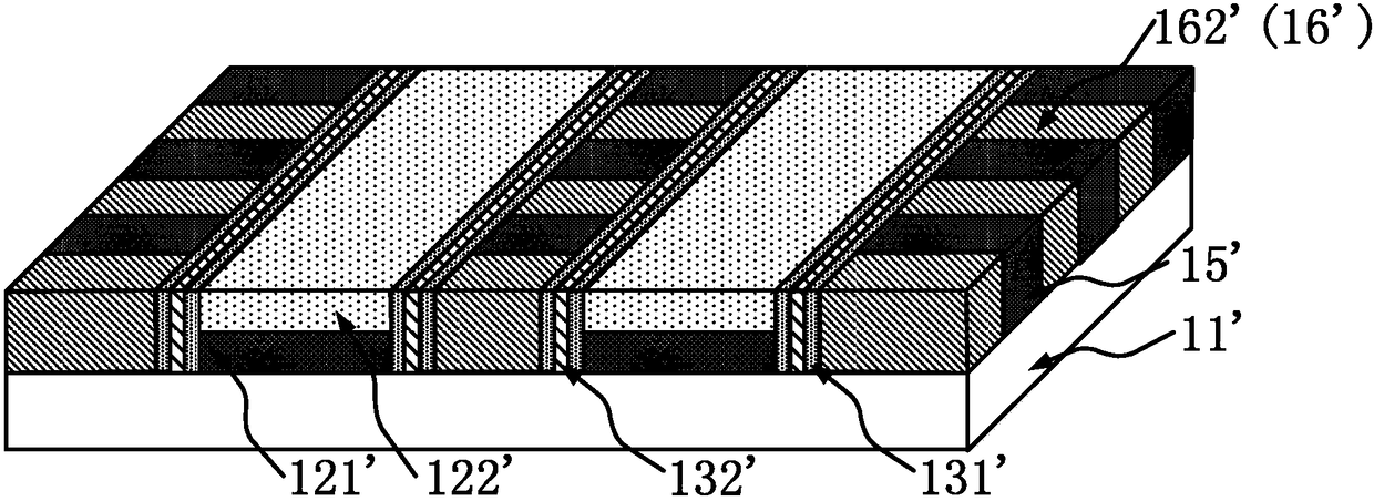
[0155] Executing step S2 , forming gate insulating sidewalls 13 and sacrificial sidewalls 140 on the sidewalls of the gate structure in sequence, and two adjacent sacrificial sidewalls 140 enclose a first groove 151 .

[0156] Step S3 is executed, forming a plug conductive layer 150 in the first groove 151 surrounded by the sacrificial sidewall 140 , and forming a plurality of plug conductive structures 15 isolated by a plurality of second grooves 161 by etching.

[0157] The specific implementation manners o...


PUM


Abstract

The invention discloses a semiconductor transistor preparation method and structure. The structure comprises a semiconductor substrate; a gate structure arranged on the upper surface of the semiconductor substrate and comprising a gate conductive layer and a gate insulation layer arranged on the gate conductive layer; gate insulation side walls arranged at the side walls of the gate structure; bolt conductive structures arranged at the two sides of the gate structure, wherein the bolt conductive structures are electrically isolated through an air insulation structure or an insulation layer; and air side walls arranged between bolt conductive layers and the gate insulation side walls. Each air side wall comprises an air gap and an insulated seal layer, wherein the air gap is sealed by the insulated seal layer. Compared with the prior art, through introduction of the air gaps and air gap chambers, not only parasitic capacitance between grid electrodes and the bolt conductive structures is reduced, but also parasitic capacitance between the bolt conductive structure and the bolt conductive structure is reduced, thereby improving stability and reliability of a transistor, and providingan effective means for further reducing the size of the transistor.

Description

technical field [0001] The invention relates to a manufacturing process of a semiconductor device, in particular to a manufacturing method and structure of a semiconductor transistor. Background technique [0002] A Metal-Oxide-Semiconductor Field-Effect Transistor (MOSFET, Metal-Oxide-Semiconductor Field-Effect Transistor) is the most commonly used unit in an integrated circuit. Since the voltages of the gate, source and drain of the MOSFET are not equal under normal working conditions, there is a coupling effect in the electric field between them, and this coupling effect is manifested as the existence of capacitance between them. With the development of integrated circuits, the miniaturization of devices is an inevitable trend, but the parasitic capacitance in the process does not decrease proportionally with the reduction of device size, while the intrinsic capacitance decreases proportionally with the reduction of device size , so that the proportion of parasitic capac...

Claims


Application Information

Patent Timeline
Patent Type & Authority Applications(China)
IPC IPC(8): H01L21/8232H01L27/088H01L21/768
CPCH01L27/088H01L21/7682H01L21/76835H01L21/823468H01L2221/1047
Inventor 不公告发明人
Owner CHANGXIN MEMORY TECH INC
Why Eureka
Try Eureka