Trenched mosfets with embedded schottky in the same cell

a technology of mosfet and trench schottky, which is applied in the direction of diodes, basic electric elements, electric devices, etc., can solve the problems of trench schottky diodes occupying about the same space as the mosfet, increasing the cost and process complications of producing the mosfet power devices, and further suffering from a high leakage between the drain and the sour

Inactive Publication Date: 2008-10-09
FORCE MOS TECH CO LTD
View PDF8 Cites 116 Cited by
  • Summary
  • Abstract
  • Description
  • Claims
  • Application Information

AI Technical Summary

Benefits of technology

[0009]It is therefore an aspect of the present invention to provide new and improved semiconductor power device configuration and manufacture processes for providing semiconductor power devices with embedded Schottky diode such that space occupied by separate Schottky diodes can be saved and one of the major technical limitations discussed above can be overcome.

Problems solved by technology

The configuration as disclosed in the patented invention has a disadvantage that the Schottky diodes occupy additional space that is about the same space as the MOSFET.
The trench Schottky diodes further suffer from a high leakage between the drain and source due to the increase in the phosphorus dopant concentration in the channel region during the sacrificial and gate oxidation processes.
Also, the formation process requires additional contact mask for the Schottky diode thus increases the cost and processes complications for producing the MOSFET power device with Schottky diode.
Again, the configuration has the same disadvantage that the Schottky diodes occupy additional space thus limiting the further miniaturization of the device.
Furthermore, the manufacturing cost is increased due to the requirement that an additional P+ mask is required to form the Schottky diodes.

Method used


Image

  • Trenched mosfets with embedded schottky in the same cell
  • Trenched mosfets with embedded schottky in the same cell
  • Trenched mosfets with embedded schottky in the same cell

Examples


Embodiment Construction

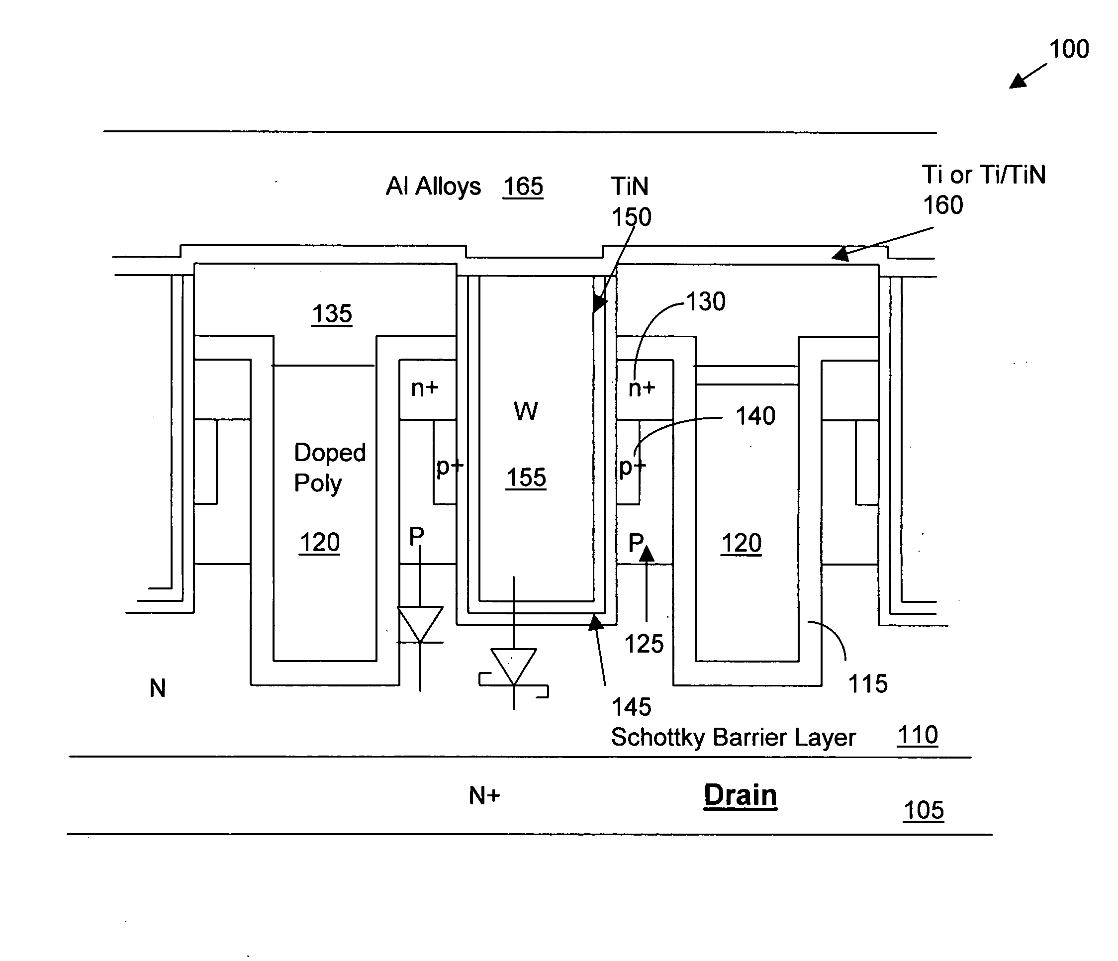
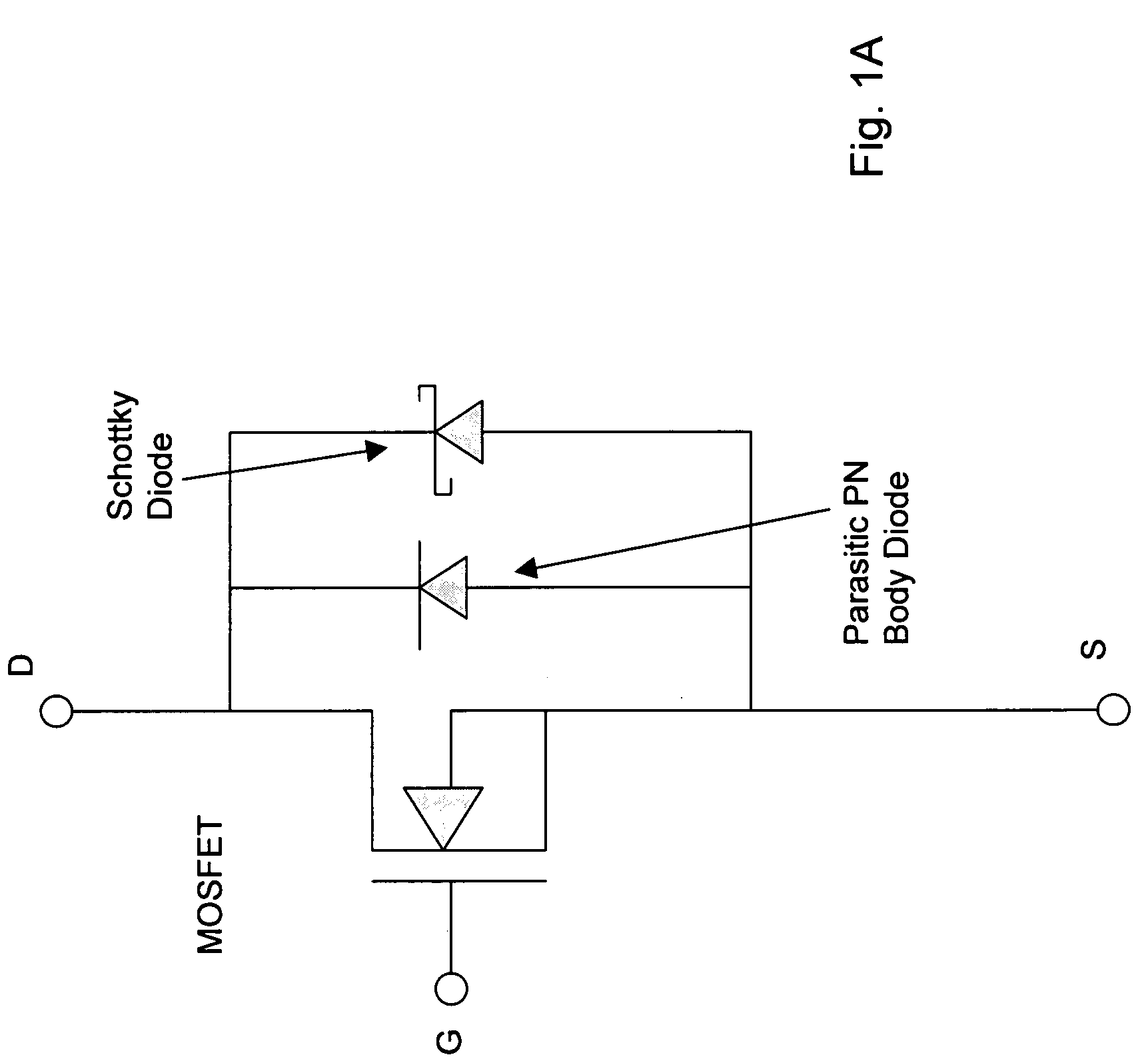
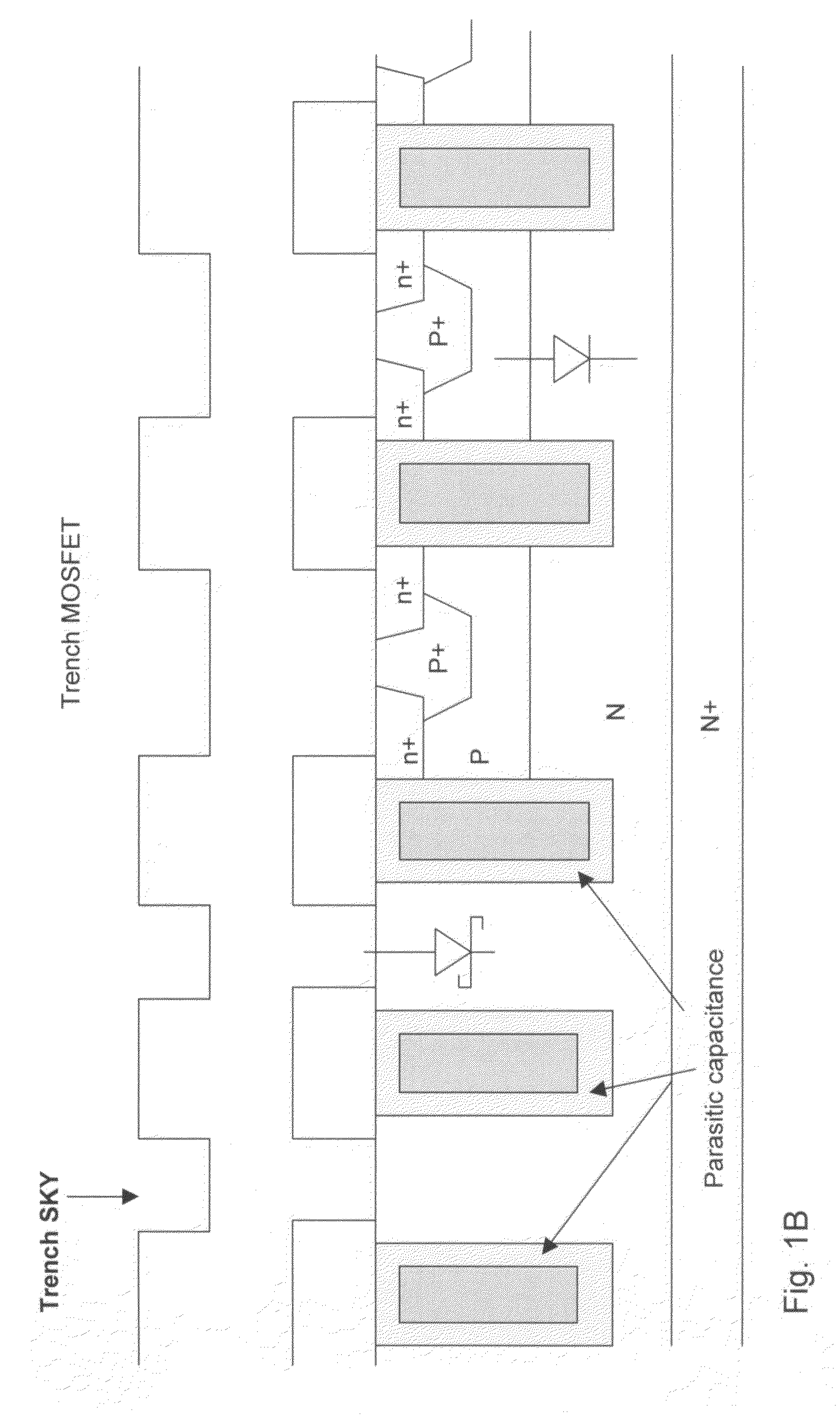
[0019]Please refer to FIG. 2 shows a side cross-sectional view of a trench MOSFET 100 with embedded Schottky in the same cell of this invention. The trenched MOSFET 100 is supported on a substrate 105 formed with an epitaxial layer 110. The MOSFET device 100 includes trenched gates 120 disposed in a trench with a gate insulation layer 115 formed over the walls of the trench. A body region 125 that is doped with a dopant of second conductivity type, e.g., P-type dopant, extends between the trenched gates 120. The P-body regions 125 encompassing a source region 130 doped with the dopant of first conductivity, e.g., N+ dopant. The source regions 130 are formed near the top surface of the epitaxial layer surrounding the trenched gates 120. The trench MOSFET device includes an embedded Schottky formed near the bottom of the trench contact filled with a tungsten plug 155. The Schottky diodes are formed in the contact trench with a CoSi2 / TiN layer 145 and a barrier layer 150 underneath the...


PUM


Abstract

A semiconductor power device includes trenched semiconductor power device comprising a trenched gate surrounded by a source region encompassed in a body region above a drain region disposed on a bottom surface of a substrate. The semiconductor power device further includes an insulation layer covering the trenched semiconductor power device with a source-body contact trench opened therethrough the source and body regions and extending into an epitaxial layer below the body regions and filled with contact metal plug therein. The semiconductor power device further includes an embedded Schottky diode disposed near a bottom of the source-body contact trench below the contact metal plug wherein the Schottky diode further includes a Schottky barrier layer having a barrier height for reducing a leakage current through the embedded Schottky diode during a reverse bias between the drain and the source.

Description

BACKGROUND OF THE INVENTION[0001]1. Field of the Invention[0002]This invention relates generally to the cell structure, device configuration and fabrication process of power semiconductor devices. More particularly, this invention relates to a novel and improved cell configuration and processes to manufacture MOSFET device with embedded Schottky diodes in the same cell such that integrated cells with spacing savings and lower capacitance and higher performance are achieved.[0003]2. Description of the Related Art[0004]Conventional technologies for high efficiency DC / DC applications, a Schottky diode is usually added externally in parallel to a semiconductor power device, e.g., a power MOSFET device. FIG. 1A is a circuit diagram that illustrates the implementation of a Schottky with a power MOSFET device. The Schottky diode (SKY) is connected in parallel to the MOSFET device with a parasitic PN body diode to function as a clamping diode to prevent the body diode from turning on. In or...

Claims


Application Information

Patent Timeline
Patent Type & Authority Applications(United States)
IPC IPC(8): H01L29/78H01L21/336
CPCH01L21/26586H01L29/0878H01L29/1095H01L29/41766H01L29/42368H01L29/456H01L29/47H01L29/66727H01L29/66734H01L29/7806H01L29/7813
Inventor HSHIEH, FWU-IUAN
Owner FORCE MOS TECH CO LTD
Why Eureka
Try Eureka