Method for forming active pillar of vertical channel transistor

a vertical channel transistor and active pillar technology, applied in the field of semiconductor device technology, can solve the problems of increasing the difficulty of subsequent process, reducing the line width of the active pillar b>100, etc., and achieve the effect of reducing the horizontal width of the mask pattern

Active Publication Date: 2010-03-04
SK HYNIX INC
View PDF5 Cites 205 Cited by
  • Summary
  • Abstract
  • Description
  • Claims
  • Application Information

AI Technical Summary

Benefits of technology

[0012]In accordance with an aspect of the present invention, there is provided a method for forming a pillar of a vertical channel transistor, including: forming a mask pattern over a substrate; vertically etching the substrate using the mask pattern as an etch barrier to form a pillar; horizontally etching the vertically etched sub

Problems solved by technology

However, limitation exists on reducing the line width of the active pillar 100A due to a defined photolithography process.
As aforementioned, when the sidewalls of the active pil

Method used


Image

  • Method for forming active pillar of vertical channel transistor
  • Method for forming active pillar of vertical channel transistor
  • Method for forming active pillar of vertical channel transistor

Examples


Embodiment Construction

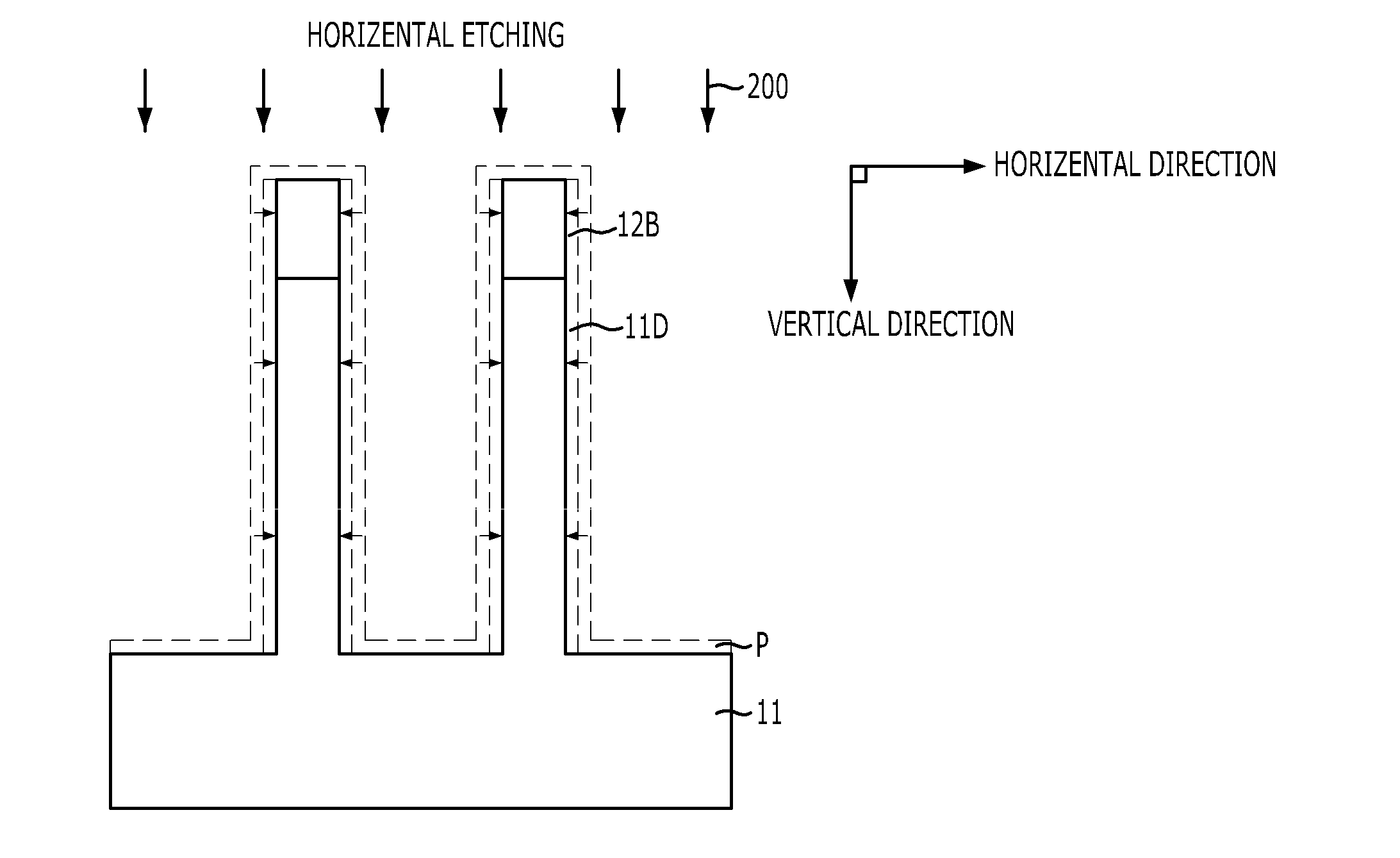
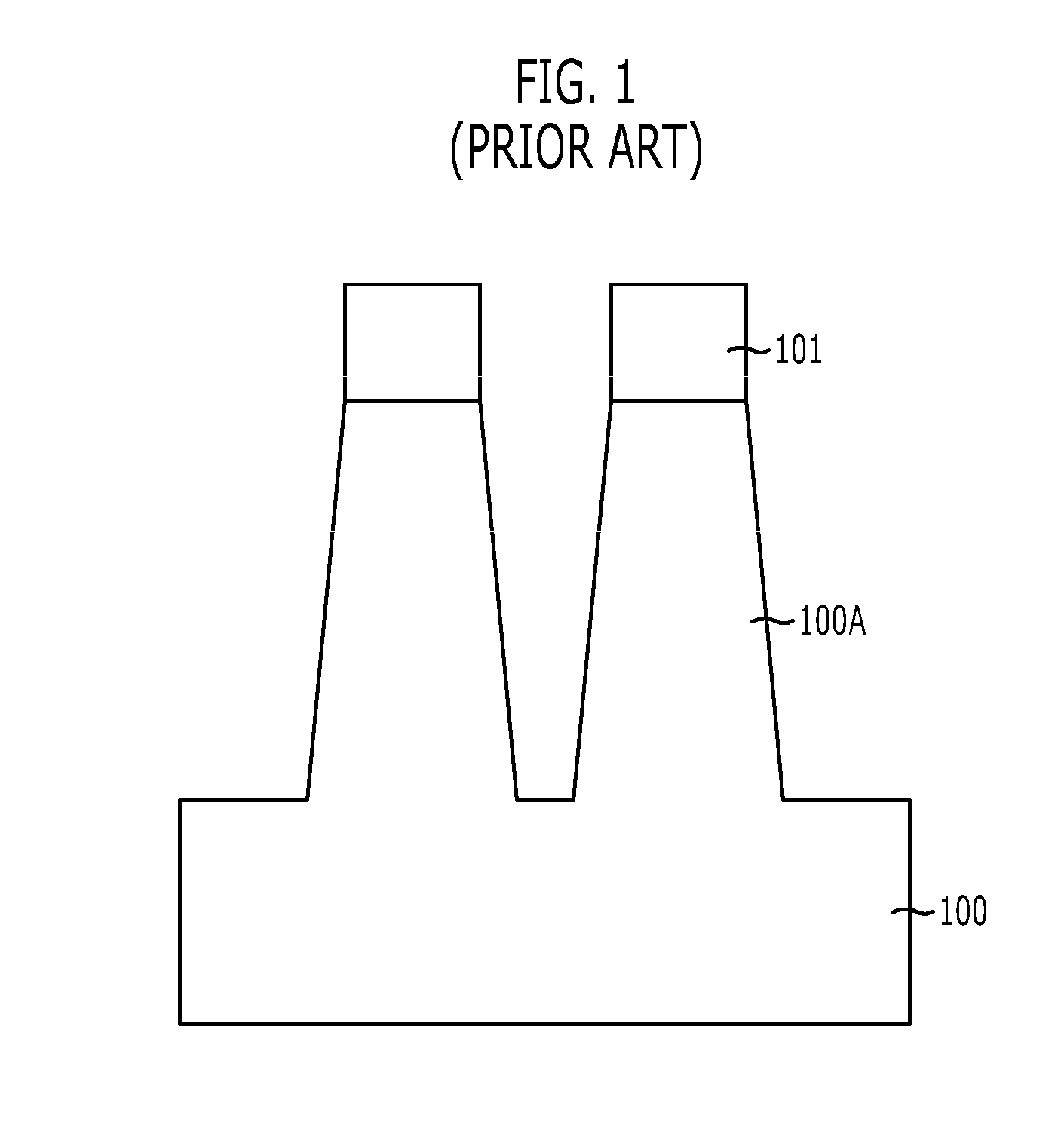
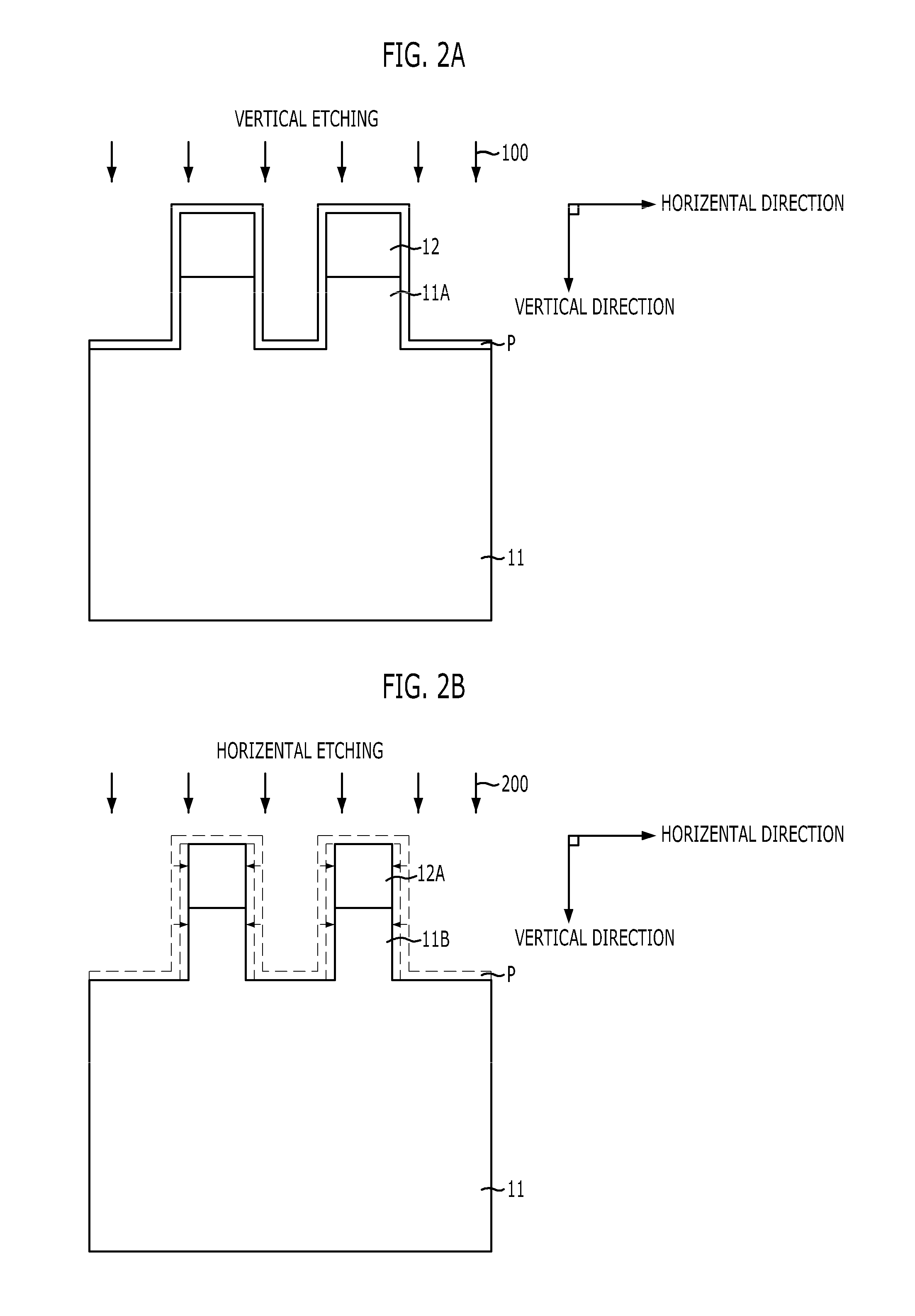
[0016]Other objects and advantages of the present invention can be understood by the following description, and become apparent with reference to the embodiments of the present invention. In the figures, the dimensions of layers and regions are exaggerated for clarity of illustration. It will also be understood that when a layer (or film) is referred to as being ‘on’ another layer or substrate, it can be directly on the other layer or substrate, or intervening layers may also be present. Furthermore, it will be understood that when a layer is referred to as being ‘under’ another layer, it can be directly under, and one or more intervening layers may also be present. In addition, it will also be understood that when a layer is referred to as being ‘between’ two layers, it can be the only layer between the two layers, or one or more intervening layers may also be present. Embodiments of the invention are described hereafter with reference to the accompanying drawings.

[0017]The embodim...


PUM


Abstract

A method for forming an active pillar of a vertical channel transistor includes forming a hard mask pattern on a substrate, etching vertically the substrate using the hard mask pattern as an etch barrier to form an active pillar, and etching horizontally to remove by-product remaining on the exposed substrate, the hard mask pattern and the active pillar and at the same time to reduce line width of the hard mask pattern and the active pillar, wherein a unit cycle in which the vertical etching and the horizontal etching are each performed subsequently once, respectively, is performed repeatedly at least two times or more. According to the present invention, an active pillar having vertical profiles on its sidewalls and having height and line width (or diameter) required in a highly integrated vertical channel transistor can be provided.

Description

CROSS-REFERENCE TO RELATED APPLICATIONS[0001]The present invention claims priority of Korean patent application number 10-2008-0086309 filed on Sep. 2, 2008, respectively, the disclosure of which is incorporated herein by reference in its entirety.BACKGROUND OF THE INVENTION[0002]The present invention relates to a technology of fabricating a semiconductor device, and more particularly, to a method for forming active pillars of a vertical channel transistor.[0003]Recently, a semiconductor memory device having 4F2 (F: minimum feature size) has been demanded as the size of a semiconductor device decreases, and thus a semiconductor device provided with a vertical channel transistor has been proposed. The vertical channel transistor is configured such that a surround type gate surrounding a periphery of an active pillar extending vertically on a substrate is formed and then a drain region and a source region are formed on upper end and lower end of the active pillar, respectively, around...

Claims


Application Information

Patent Timeline
IPC IPC(8): H01L21/306
CPCH01L21/30655H01L21/3065H01L29/66666H01L29/7827
Inventor KIM, MYUNG-OK
Owner SK HYNIX INC
Why Eureka
Try Eureka